CDP1879 View Datasheet(PDF) - Intersil
Part Name
Description
View to exact match
CDP1879 Datasheet PDF : 18 Pages
| |||
CDP1879, CDP1879C-1
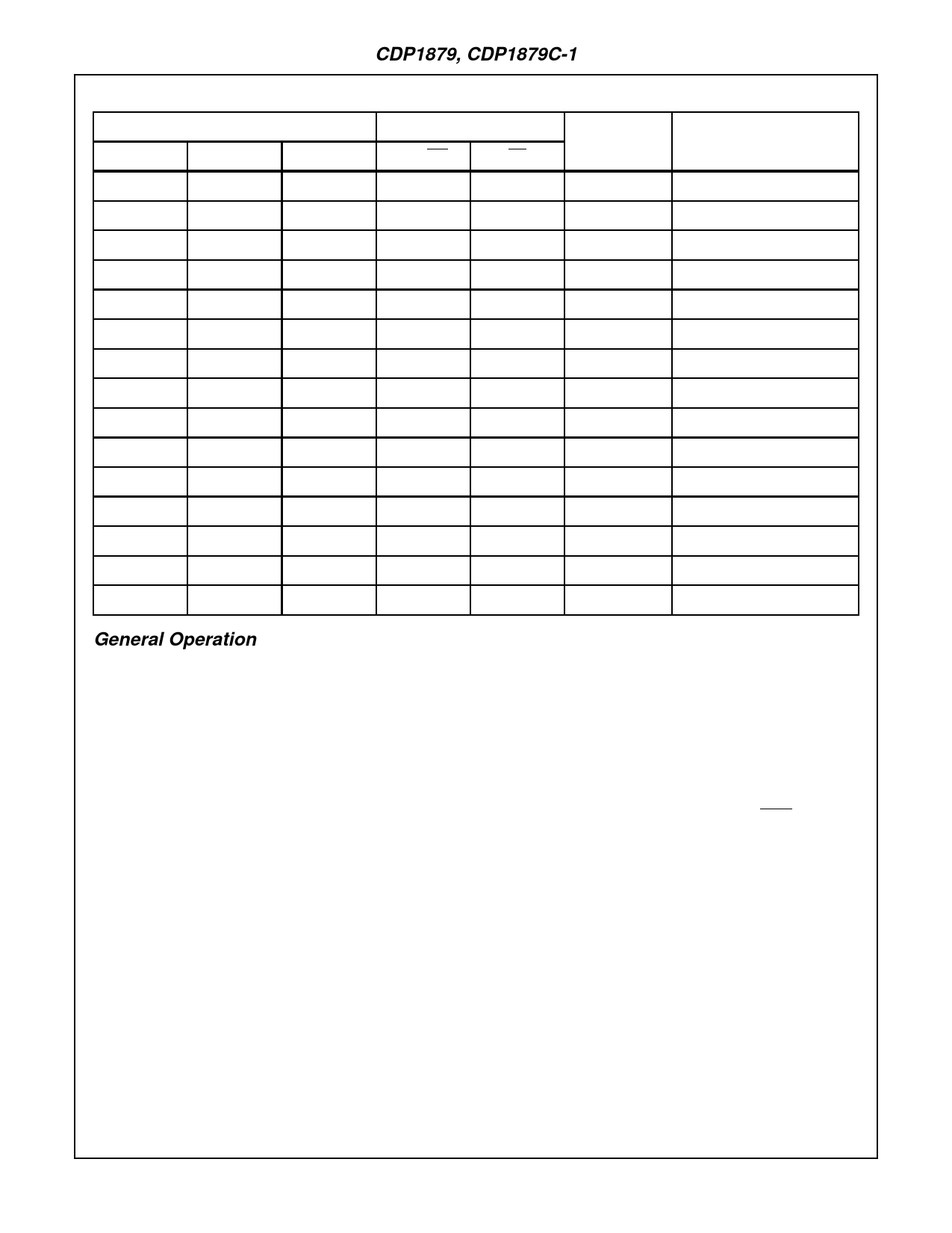
ADDRESS
A2
A1
AO
0
1
0
0
1
0
0
1
1
0
1
1
1
0
0
1
0
0
1
0
1
1
0
1
1
1
0
1
1
0
0
1
0
0
1
1
1
0
0
1
1
1
1
1
1
REGISTER TRUTH TABLE
ACTIVE SIGNAL
TPB/WR
RD
BIT 3 CONTROL
REGISTER
REGISTER OPERATION
X
-
0
Write Seconds Counter
-
X
0
Read Seconds Counter
X
-
0
Write Minutes Counter
-
X
0
Read Minutes Counter
X
-
0
Write Hours Counter
-
X
0
Read Hours Counter
X
-
0
Write Date Counter
-
X
0
Read Date Counter
X
-
0
Write Month Counter
-
X
0
Read Month Counter
X
-
1
Write Seconds Alarm Latch
X
-
1
Write Minutes Alarm Latch
X
-
1
Write Hours Alarm Latch
X
-
-
Write Control Register
-
X
-
Read Int. Status Register
General Operation
The real-time clock contains seconds, minutes, and hours,
date and month counters that hold time of day/calendar
information (see Figure 2). The frequency of an intrinsic
oscillator is divided down to supply a once-a-second signal
to the counter series string. The counters are separately
addressable and can be written to or read from.
The real-time clock contains seconds, minutes and hour
write-only alarm latches that store the alarm time (see Fig-
ure 3). When the value of the alarm latches and counters are
equal, the interrupt output is activated. The interrupt output
can also be activated by a clock output transition. The clock
output is derived from the prescaler and counters and can
be one of 15 square-wave signals. The value in the read-
only interrupt status register identifies the interrupt source.
Operational control of the real-time clock is determined by
the byte in a write-only control register. The 8-bit value in this
register determines the correct divisor for the prescaler, a
data direction and alarm enable bit, clock output select, and
start/stop control (see Figure 4).
Data transfer and addressing are accomplished in two
modes of operation, memory mapping and I/O mapping
using the CDP1800-series microprocessors. The mode is
selected by the level on an input pin. (IO/MEM). Memory
mapping implies use of the address lines as chip selects and
address inputs during linear selection or partial or full decod-
ing methods. I/O mapping with the CDP1800-series micro-
processors involves use of the N line outputs in conjunction
with input and output instructions to transfer data to and from
memory.
4-109
Share Link: 