CDP1879 View Datasheet(PDF) - Intersil
Part Name
Description
View to exact match
CDP1879 Datasheet PDF : 18 Pages
| |||
CDP1879, CDP1879C-1
upper two bits of the interrupt status register identify the
interrupt source. The interrupt status register has the same
address as the control register. Addressing the interrupt sta-
tus register with the RD line active will place these register
bits on the data bus. Bits 0-5 are held low. A “1” in bit-6 rep-
resents a clock output transition as the interrupt source. A
“1” in bit-7 will identify the alarm circuit as the interrupt
source.
Activating the reset pin (active low) resets the hour latch to
“30” which prevents a match between alarm and time regis-
ters during an initialization procedure. Activating the reset
pin or writing to the control register resets the interrupt out-
put (high) and clears the interrupt status register
Clock Output
One of 15 counter and prescaler overflows can be selected
as a 50% duty cycle output signal that is available at the
“clock out” pin. The frequency is selected by the upper nibble
in the control register. For example, selecting a one-second
clock output will result in a repetitive signal that will be high
for 500ms and low for the same period. The high-to-low tran-
sition of the output signal will set the clock bit in the status
register and activate the interrupt output. The level of the
“clock out” signal is derived from the value in the counter.
Example - if hours clock is selected and the minutes counter
holds 4 minutes, the clock out will be low for 26 minutes and
high for 30 minutes Thereafter, the clock out will toggle at a
50% duty cycle rate (see Table 1 and Figure 3).
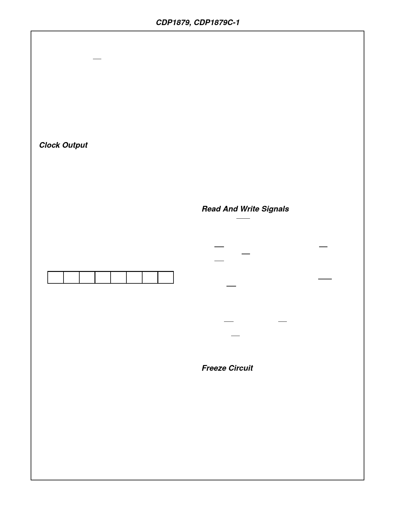
CONTROL REGISTER (SEE TABLE 1 AND FIGURE 4)
BIT
BIT
7
6
5
4
3
2
1
0
CONTROL REGISTER BYTE
The 8-bit value in the control register determines the follow-
ing:
1. Bit 0 and 1 - Frequency Select - Since there are one of 4
possible crystals the oscillator in the real-time clock can
operate with, these bit levels determine the prescaler divi-
sor so that an accurate one second pulse is supplied to
the counter series string.
BIT 1
0
0
1
1
BIT 0
0
1
0
1
FREQUENCY
32,768Hz
1.048576MHz
2.097152MHz
4.194304MHz
2. Bit 2 - Start-Stop Control - Counter enabling is controlled
by the value at this location. A “1” will allow the counters
to function and a “0” in this location will disable the
counters.
3 Bit 3 - Counter/Latch Control - The level at this location
controls two functions. It is required since the counters
and alarm latches have the same addresses.
1) A “0” in bit-3 will direct subsequent data to or from
the counter selected and the alarm function will be
disabled.
2) A “1” in bit-3 will direct subsequent data to or from
the alarm latch and will enable the alarm.
4. Bits 4 to 7 - Clock Select - These bits select one of 15
square-wave signals that will be present at the “clock-
out” pin. If bit-4 to bit-7 are zero's, the clock output pin will
be high. If a clock is selected, the first high-to-low clock
out transition will activate the interrupt pin (active low) and
place a “1” in bit-6 of the status register. Writing to the
control register or activating the reset pin will set the inter-
rupt pin high and reset the interrupt status register.
Normal operation requires the control register to be written
to and loaded first with a control word. However, subsequent
writing to a counter if a “clock out” is selected may cause an
interrupt out signal. Therefore, “clock-out” should be dese-
lected by writing zero's into bit-4 through bit-7 if the interrupt
is used. When the counters are loaded, the control register
is again written to with the value in the upper nibble selecting
the “clock out” signal. See Table 1.
Read And Write Signals
When the IO/MEM pin is low, the real-time clock is enabled
for memory mapped operation. Data on the bus is placed in,
or read from a counter, alarm latch or register by 1) placing
the CS pin high, 2) selective addressing, 3) placing the
TPB/WR pin low during a write cycle with the RD pin high or
4) setting the RD pin low during a read cycle with this
TPB/WR pin high.
The I/O mapping mode used with the CDP1800 series
microprocessor is selected by setting the IO/MEM pin high.
The TPB/WR pin on the real-time clock is connected to the
TPB output pin of the microprocessor. Data on that bus is
written to or read from the counters, latches and registers by
1) placing the CS pin high, 2) selective addressing utilizing
the microprocessor N lines and I/O instructions, 3) placing
the TPB/WR pin high with the RD pin low during an output or
write operation (data is latched on TPB's trailing edge), 4)
setting the RD line high during an input or read operation.
Data is placed on the bus by the real-time clock between the
trailing edges of TPA and TPB.
Freeze Circuit
Since writing to or reading from the counters or alarm
latches is performed asynchronously, the once-a-second
signal from the prescaler may pulse the counter series string
during these operations. This can result in erroneous data.
To avoid this occurring, a transparent “freeze” circuit' is incor-
porated into the real-time clock. This circuit is designed to
trap and hold the one-second input clock transition if it
occurs during access times. When the operations are com-
pleted, it is inserted into the counter series string. To utilize
the “freeze” circuit, address “1” (A0 = 1, A1 = 0, A2 = 0) is
selected first while performing a write operation. Read or
write accesses may now be performed with assurance the
data is stable. All operations must be concluded within
4-113
Share Link: 