TC58NS256DC View Datasheet(PDF) - Toshiba
Part Name
Description
View to exact match
TC58NS256DC Datasheet PDF : 33 Pages
| |||
TC58NS256DC
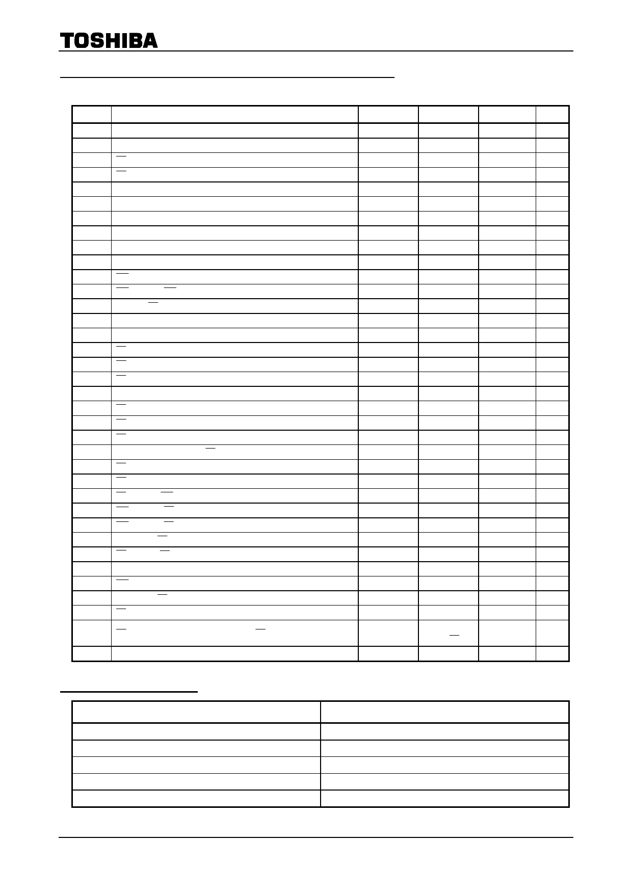
AC CHARACTERISTICS AND OPERATING CONDITIONS
(Ta = 0°~55°C, VCC = 3.3 V ± 0.3 V)
SYMBOL
PARAMETER
MIN
tCLS
CLE Setup Time
0
tCLH
CLE Hold Time
10
tCS
CE Setup Time
0
tCH
CE Hold Time
10
tWP
Write Pulse Width
25
tALS
ALE Setup Time
0
tALH
ALE Hold Time
10
tDS
Data Setup Time
20
tDH
Data Hold Time
10
tWC
Write Cycle Time
50
tWH
WE -High Hold Time
15
tWW
WP High to WE Low
100
tRR
Ready-to- RE Falling Edge
20
tRP
Read Pulse Width
35
tRC
Read Cycle Time
50
tREA
RE Access Time (Serial Data Access)
tCEH
CE -High Time for Last Address in Serial Read Cycle
100
tREAID RE Access Time (ID Read)
tOH
Data Output Hold Time
10
tRHZ
RE -High-to-Output-High Impedance
tCHZ
CE -High-to-Output-High Impedance
tREH
RE -High Hold Time
15
tIR
Output-High-Impedance-to- RE Rising Edge
0
tRSTO
RE Access Time (Status Read)
tCSTO
CE Access Time (Status Read)
tRHW
RE High to WE Low
0
tWHC
WE High to CE Low
30
tWHR
WE High to RE Low
30
tAR1
ALE Low to RE Low (ID Read)
100
tCR
CE Low to RE Low (ID Read)
100
tR
Memory Cell Array to Starting Address
tWB
WE High to Busy
tAR2
ALE Low to RE Low (Read Cycle)
50
tRB
RE Last Clock Rising Edge to Busy (in Sequential Read)
tCRY
CE High to Ready (When interrupted by CE in Read Mode)
tRST
Device Reset Time (Read/Program/Erase)
MAX
35
35
30
20
35
45
25
200
200
600 + tr
( RY/BY )
6/10/500
UNIT
ns
ns
ns
ns
ns
ns
ns
ns
ns
ns
ns
ns
ns
ns
ns
ns
ns
ns
ns
ns
ns
ns
ns
ns
ns
ns
ns
ns
ns
ns
µs
ns
ns
ns
ns
µs
NOTES
(2)
(1)
AC TEST CONDITIONS
PARAMETER
Input level
Input pulse rise and fall time
Input comparison level
Output data comparison level
Output load
VALUES
2.4 V, 0.4 V
3 ns
1.5 V, 1.5 V
1.5 V, 1.5 V
CL (100 pF) + 1 TTL
2000-08-27 4/33
Share Link: 