TC58NS256DC View Datasheet(PDF) - Toshiba
Part Name
Description
View to exact match
TC58NS256DC Datasheet PDF : 33 Pages
| |||
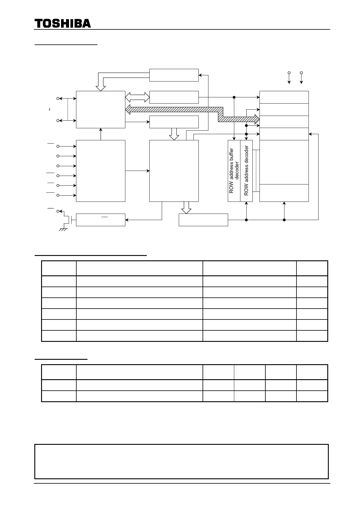
BLOCK DIAGRAM
I/O1
I/O8
CE
CLE
ALE
WE
RE
WP
RY/BY
I/O control circuit
Logic control
RY/BY
Status register
Address register
Command register
Control circuit
HV generator
TC58NS256DC
VCC VSS
Column buffer
Column decoder
Data register
Sense amp
Memory cell array
Extended area
(embedded ID)
ABSOLUTE MAXIMUM RATINGS
SYMBOL
PARAMETER
VCC
Power Supply Voltage
VIN
Input Voltage
VI/O
Input/Output Voltage
PD
Power Dissipation
Tstg
Storage Temperature
Topr
Operating Temperature
RATING
−0.6~4.6
−0.6~4.6
−0.6 V~VCC + 0.3 V (≤ 4.6 V)
0.3
−20~65
0~55
CAPACITANCE *(Ta = 25°C, f = 1 MHz)
SYMBOL
PARAMETER
CONDITION
MIN
CIN
Input
VIN = 0 V
COUT
Output
VOUT = 0 V
* This parameter is periodically sampled and is not tested for every device.
MAX
10
10
UNIT
V
V
V
W
°C
°C
UNIT
pF
pF
000707EBA2
• The products described in this document are subject to the foreign exchange and foreign trade laws.
• The information contained herein is presented only as a guide for the applications of our products. No responsibility is assumed by
TOSHIBA CORPORATION for any infringements of intellectual property or other rights of the third parties which may result from its
use. No license is granted by implication or otherwise under any intellectual property or other rights of TOSHIBA CORPORATION or
others.
• The information contained herein is subject to change without notice.
2000-08-27 2/33
Share Link: 