CDP1852 View Datasheet(PDF) - Intersil
Part Name
Description
View to exact match
CDP1852 Datasheet PDF : 9 Pages
| |||
CDP1852, CDP1852C
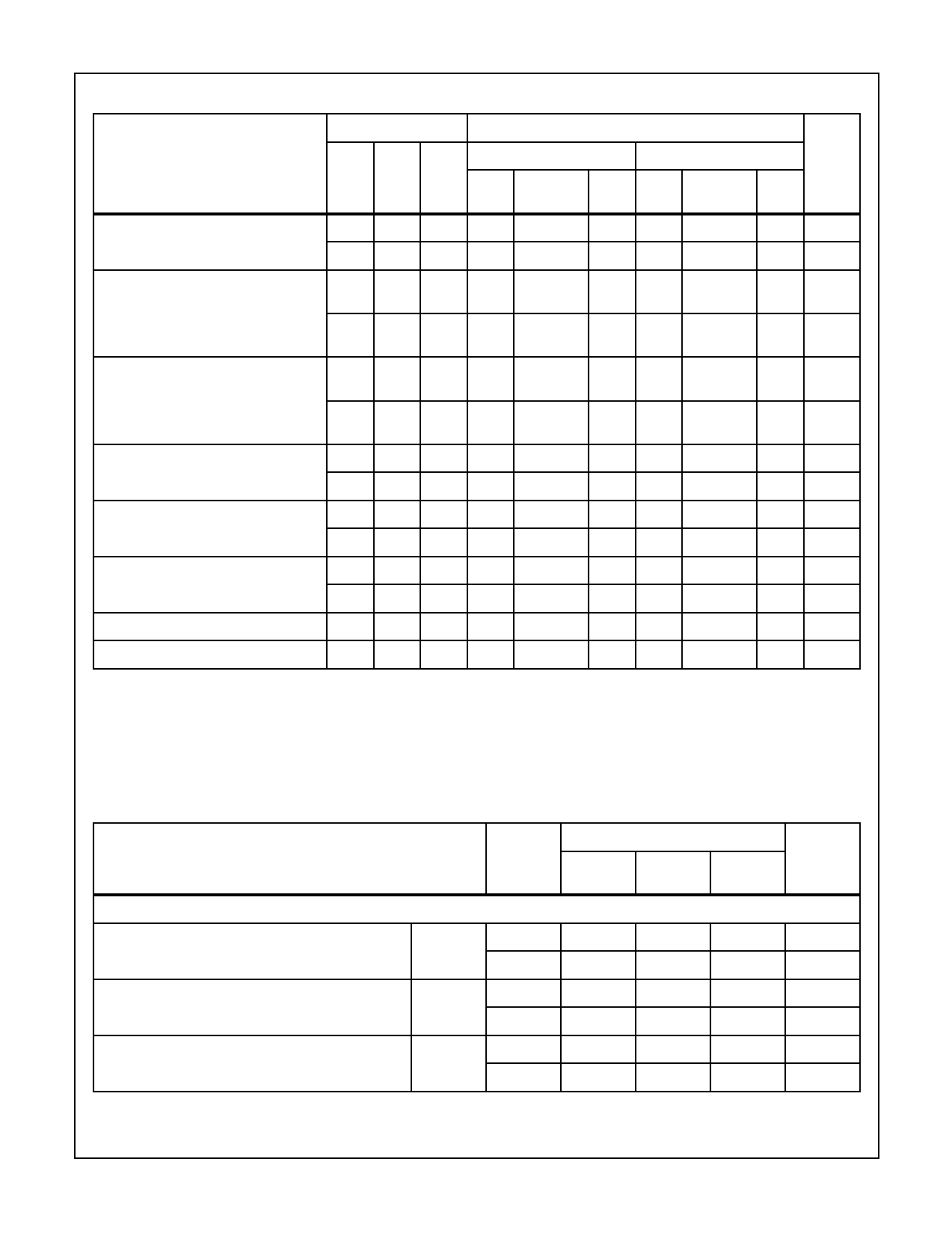
Static Electrical Specifications At TA = -40oC to +85oC, Unless Otherwise Specified (Continued)
CONDITIONS
LIMITS
CDP1852
CDP1852C
PARAMETER
VO
VIN
VDD
(NOTE1)
(NOTE1)
(V) (V) (V) MIN
TYP
MAX MIN
TYP
MAX UNITS
Output Voltage High Level
VOH
-
0, 5
5
4.9
5
(Note 2)
- 0, 10 10 9.9
10
-
4.9
5
-
-
-
-
V
-
V
Input Low Voltage
VIL 0.5,
-
5
-
4.5
-
1.5
-
-
1.5
V
0.5,
-
10
-
-
3
-
-
-
V
9.5
Input High Voltage
VlH 0.5,
-
5
3.5
-
4.5
-
3.5
-
-
V
0.5,
-
10
7
-
-
-
-
-
V
9.5
Input Leakage Current
IlN
-
0, 5
5
-
- 0, 10 10
-
-
±1
-
-
±2
-
-
±1
µA
-
-
µA
Three-State Output Leakage
IOUT 0, 5 0, 5
5
-
Current
0, 10 0, 10 10
-
-
±1
-
-
±2
-
-
±1
µA
-
-
µA
Operating Current (Note 3)
IDD1
-
0, 5
5
-
- 0, 10 10
-
130
300
-
550
800
-
150
300
µA
-
-
µA
Input Capacitance
CIN
-
-
-
-
5
7.5
-
5
7.5
pF
Output Capacitance
COUT
-
-
-
-
5
7.5
-
-
-
pF
NOTES:
1. Typical values are for TA = 25oC and nominal VDD.
2. IOL = IOH = 1µA
3. Operating current is measured at 2MHz in an CDP1802 system with open outputs and a program of 6N55, 6NAA, 6N55, 6NAA,....
Dynamic Electrical Specifications At TA = -40oC to +85oC, VDD = ±5%, tR, tF = 20ns, VIH = 0.7 VDD, VIL = 0.3 VDD, CL = 100pF,
and 1 TTL Load
LIMITS
PARAMETER
VDD
(NOTE 1)
(V)
MIN
TYP
MAX
UNITS
MODE 0 - INPUT PORT (See Figure 4)
Minimum Select Pulse Width
tSW
5
10
-
180
360
ns
-
90
180
ns
Minimum Write Pulse Width
tWW
5
-
90
180
ns
10
-
45
90
ns
Minimum Clear Pulse Width
tCLR
5
-
80
160
ns
10
-
40
80
ns
4
Share Link: 