SST89E58RDA(2011) View Datasheet(PDF) - Silicon Storage Technology
Part Name
Description
View to exact match
SST89E58RDA Datasheet PDF : 91 Pages
| |||
A Microchip Technology Company
FlashFlex MCU
SST89E54RD2A/RDA / SST89E58RD2A/RDA
Not Recommended for New Designs
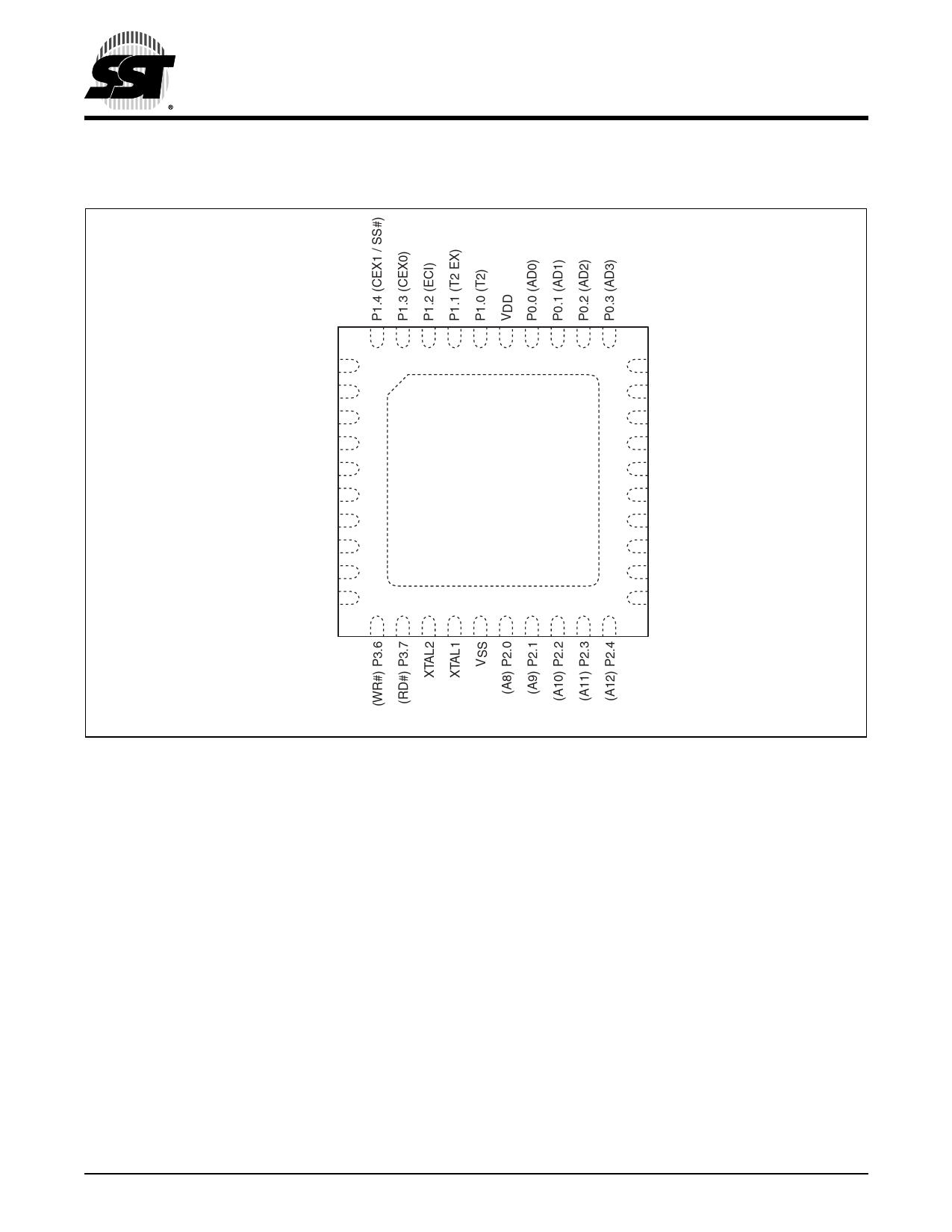
Table 1: Pin Descriptions (Continued) (2 of 3)
Symbol
P3[7:0]
P3[0]
P3[1]
P3[2]
P3[3]
P3[4]
P3[5]
P3[6]
P3[7]
PSEN#
RST
EA#
ALE/PROG#
P4[3:0]4
P4[0]
P4[1]
P4[2] / INT3#
P4[3] / INT2#
Type1
I/O with internal
pull-up
I
O
I
I
I
I
O
O
I/O
I
I
I/O
I/O with internal
pull-ups
I/O
I/O
I/O
I/O
Name and Functions
Port 3: Port 3 is an 8-bit bidirectional I/O port with internal pull-ups. The Port 3
output buffers can drive LS TTL inputs. Port 3 pins are pulled high by the inter-
nal pull-ups when “1”s are written to them and can be used as inputs in this
state. As inputs, Port 3 pins that are externally pulled low will source current
because of the internal pull-ups. Port 3 also receives some control signals and
high-order address bits during the external host mode programming and verifi-
cation.
RXD: Universal Asynchronous Receiver/Transmitter (UART) - Receive input
TXD: UART - Transmit output
INT0#: External Interrupt 0 Input
INT1#: External Interrupt 1 Input
T0: External count input to Timer/Counter 0
T1: External count input to Timer/Counter 1
WR#: External Data Memory Write strobe
RD#: External Data Memory Read strobe
Program Store Enable: PSEN# is the Read strobe to External Program
Store. When the device is executing from Internal Program Memory, PSEN# is
inactive (VOH). When the device is executing code from External Program
Memory, PSEN# is activated twice each machine cycle, except when access
to External Data Memory while one PSEN# activation is skipped in each
machine cycle. A forced high-to-low input transition on the PSEN# pin while
the RST input is continually held high for more than 20 machine cycles will
cause the device to enter External Host mode for programming.
Reset: While the oscillator is running, a high logic state on this pin for two
machine cycles will reset the device. After a reset, if the PSEN# pin is driven
by a high-to-low input transition while the RST input pin is held high, the device
will enter the External Host mode, otherwise the device will enter the Normal
operation mode.
External Access Enable: EA# must be driven to VIL in order to enable the
device to fetch code from the External Program Memory. EA# must be driven
to VIH for internal program execution. However, Security lock level 4 will disable
EA#, and program execution is only possible from internal program memory.
Address Latch Enable: ALE is the output signal for latching the low byte of
the address during an access to external memory. This pin is also the pro-
gramming pulse input (PROG#) for flash programming. Normally the ALE2 is
emitted at a constant rate of 1/6 the crystal frequency3 and can be used for
external timing and clocking. One ALE pulse is skipped during each access to
external data memory. However, if AO is set to 1, ALE is disabled.
Port 4: Port 4 is an 4-bit bi-directional I/O port with internal pull-ups. The port 4
output buffers can drive LS TTL inputs. Port 4 pins are pulled high by the inter-
nal pull-ups when ‘1’s are written to them and can be used as inputs in this
state. As inputs, port 4 pins that are externally pulled low will source current
because of the internal pull-ups.
Bit 0 of port 4
Bit 1 of port 4
Bit 2 of port 4 / INT3# External interrupt 3 input
Bit 3 of port 4 / INT2# External interrupt 2 input
©2011 Silicon Storage Technology, Inc.
8
DS25114A
12/11
Share Link: 