SST89E58RDA(2011) View Datasheet(PDF) - Silicon Storage Technology
Part Name
Description
View to exact match
SST89E58RDA Datasheet PDF : 91 Pages
| |||
A Microchip Technology Company
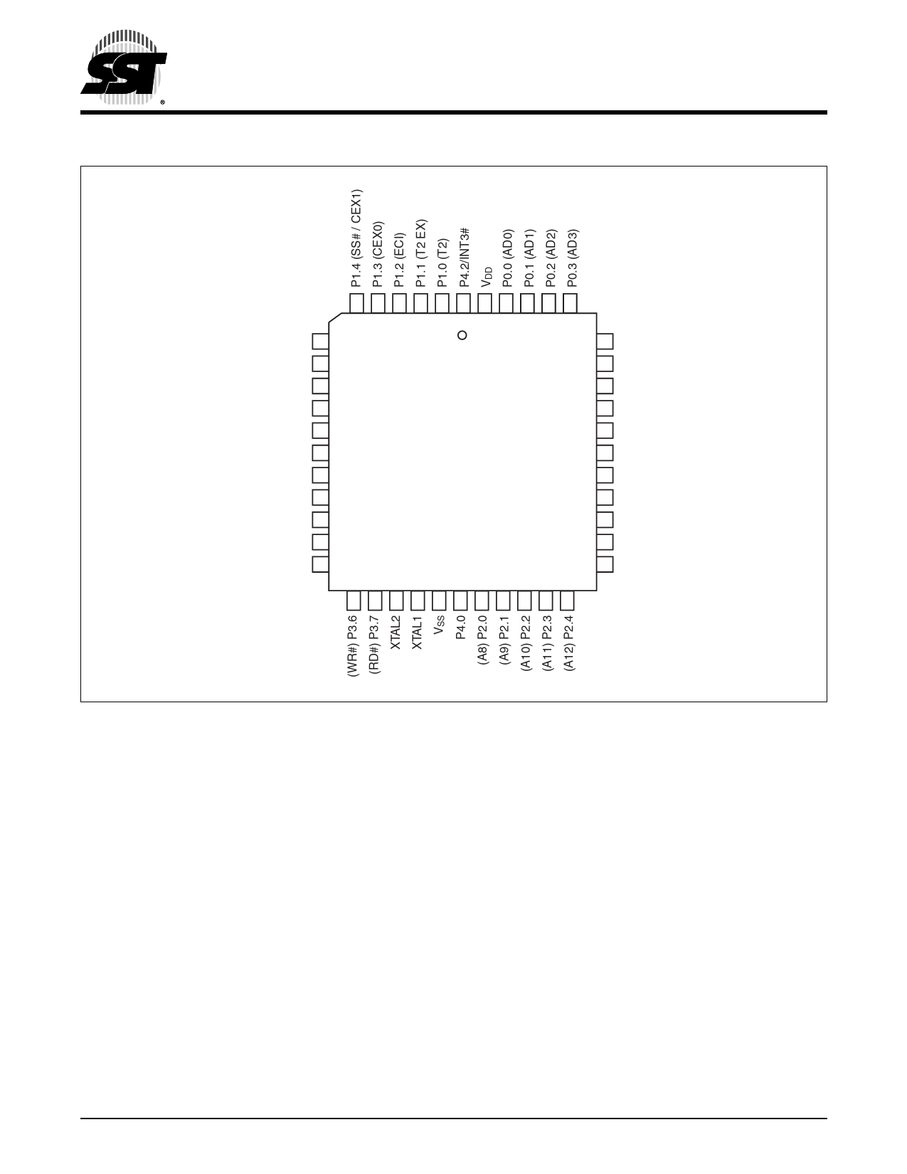
FlashFlex MCU
SST89E54RD2A/RDA / SST89E58RD2A/RDA
Memory Organization
Not Recommended for New Designs
The device has separate address spaces for program and data memory.
Program Flash Memory
There are two internal flash memory blocks in the device. The primary flash memory block (Block 0)
has 16/32 KByte. The secondary flash memory block (Block 1) has 8 KByte. Since the total program
address space is limited to 64 KByte, the SFCF[1:0] bit are used to control program bank selection.
Please refer to Figures 5 and 6 for the program memory configuration. Program bank selection is
described in the next section.
The 16K/32K x8 primary SuperFlash block is organized as 128/256 sectors, each sector consists of
128 Bytes.
The 8K x8 secondary SuperFlash block is organized as 64 sectors, each sector consists also of 128
Bytes.
For both blocks, the 7 least significant program address bits select the byte within the sector. The
remainder of the program address bits select the sector within the block.
FFFFH
EA# = 0
FFFFH
E000H
DFFFH
EA# = 1
SFCF[1:0] = 00
8 KByte
Block 1
FFFFH
E000H
DFFFH
EA# = 1
SFCF[1:0] = 01
8 KByte
Block 1
EA# = 1
SFCF[1:0] = 10, 11
FFFFH
External
64 KByte
Not
Accessible
Not
Accessible
Not
Accessible
0000H
4000H
3FFFH
2000H
1FFFH
0000H
8 KByte
Block 0
8 KByte
Block 1
4000H
3FFFH
0000H
16 KByte
Block 0
4000H
3FFFH
0000H
16 KByte
Block 0
1339 F02.0
Figure 5: Program Memory Organization for 16 KByte SST89E54RDxA
©2011 Silicon Storage Technology, Inc.
10
DS25114A
12/11
Share Link: 