SAA4952WP View Datasheet(PDF) - Philips Electronics
Part Name
Description
View to exact match
SAA4952WP Datasheet PDF : 32 Pages
| |||
Philips Semiconductors
Memory controller
Objective specification
SAA4952WP
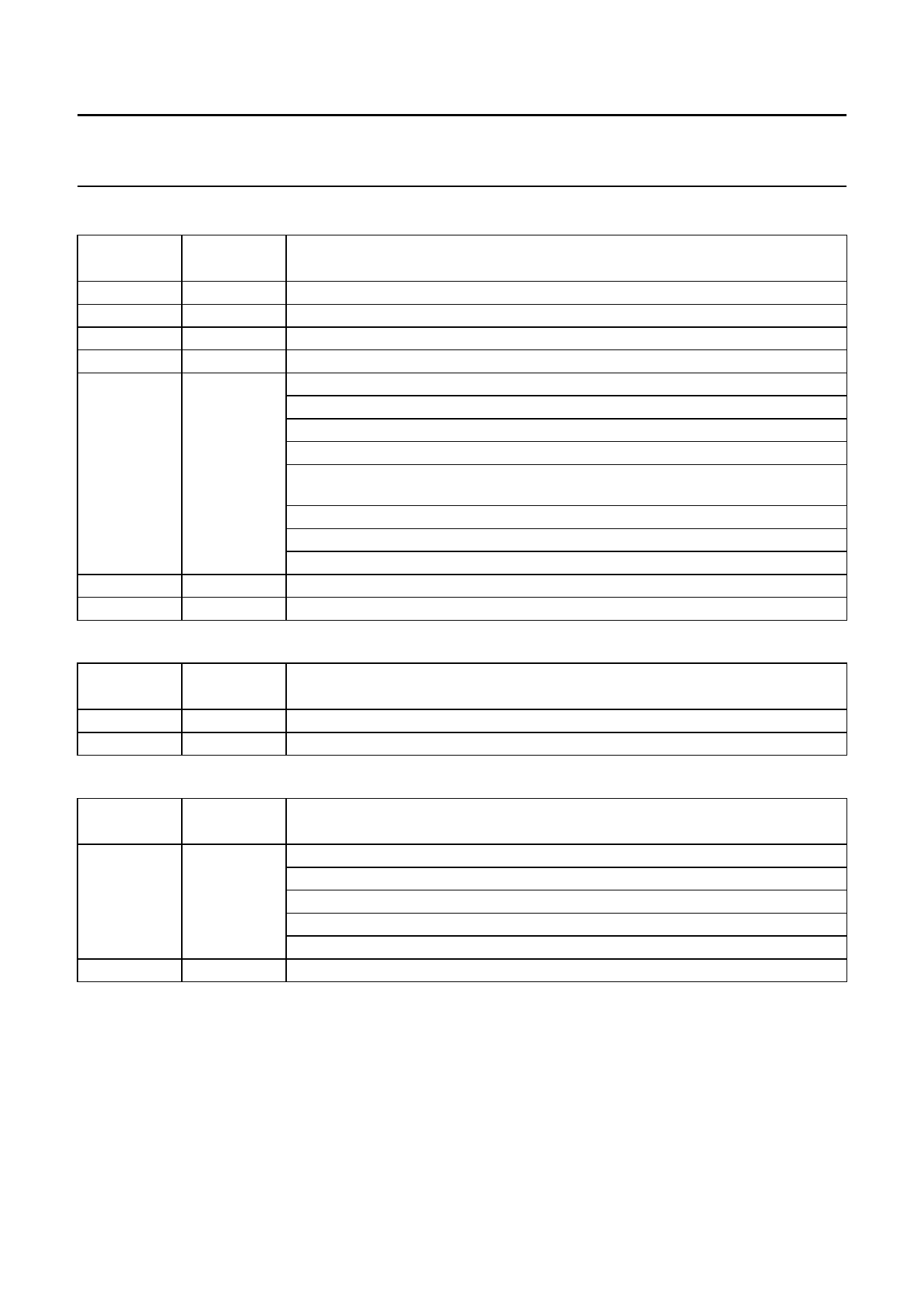
Table 4 Horizontal acquisition related pulses
ADDRESS
(HEX)
58
59
5A
5B
5C
5D
5E
REGISTER
FUNCTION
CLVSTA
CLVSTO
HWE1STA
HWE1STO
HAMSBDEL
HVACQS1
HVACQS2
start of clamp pulse
stop of clamp pulse
start of horizontal write enable 1 (lower 8 of 9 bits)
stop of horizontal write enable 1 (lower 8 of 9 bits)
bit 0: MSB of HWE1STA
bit 1: MSB of HWE1STO
bit 2: fine delay of HWE1 (LSB)
bit 3: fine delay of HWE1 (MSB)
bit 4: PWC05: Phase of Write Clock SWC05, determines the phase relationship of
SWC05 towards BLNA or HRA
bit 5: SFR: Select Field Recognition mode
bit 6: FRD: Field Recognition Disabled (FRD = 1)
bit 7: don’t care
VACQ sample pulse 1
VACQ sample pulse 2
Table 5 Mode registers
ADDRESS
(HEX)
60
61
REGISTER
MODE0
MODE1
mode register 0; see Table 7
mode register 1; see Table 10
FUNCTION
Table 6 Read registers
ADDRESS
(HEX)
81
80
REGISTER
FUNCTION
FIELDINF2
FIELDINF1
bit 0: bit 8 of field length measurement
bit 1: bit 9 of field length measurement (MSB)
bit 2: LSB of display field count
bit 3: field recognition for incoming source
bit 4: MSB of display field count
result of field length measurement (lower 8 of 10 bits)
1997 Jun 10
11
Share Link: 