M27W401-100B6TR View Datasheet(PDF) - STMicroelectronics
Part Name
Description
View to exact match
M27W401-100B6TR Datasheet PDF : 15 Pages
| |||
M27W401
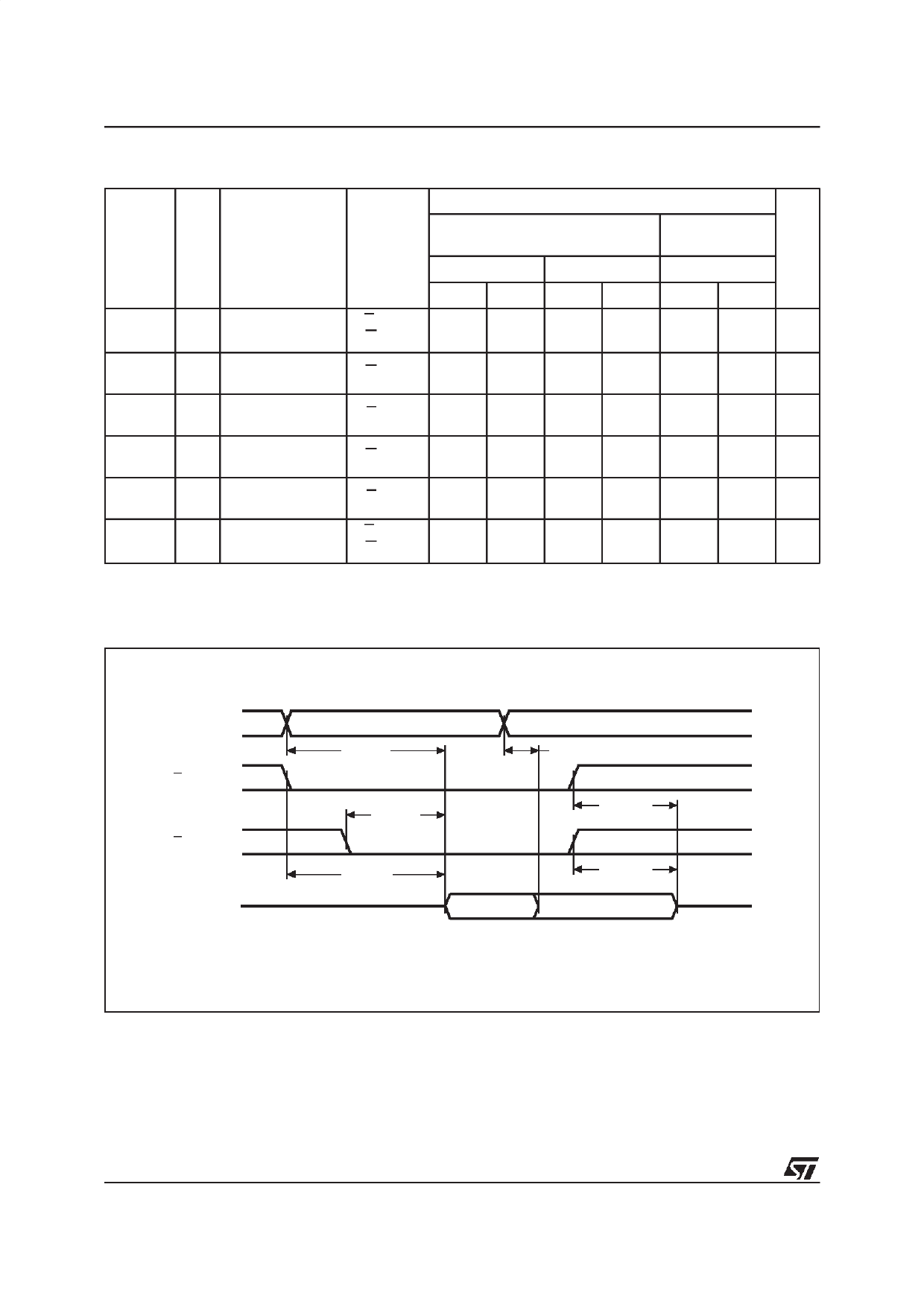
Table 8. Read Mode AC Characteristics (1)
(TA = –40 to 85°C; VCC = 2.7V to 3.6V; VPP = VCC)
M27W401
Symbol Alt
Parameter
Test
Condition
-80 (3)
-100
(-120/-150/-200)
VCC = 3.0V to 3.6V VCC = 2.7V to 3.6V VCC = 2.7V to 3.6V
Unit
Min Max Min Max Min Max
tAVQV
tACC
Address Valid to
Output Valid
E = VIL,
G = VIL
70
80
100 ns
tELQV
tCE
Chip Enable Low to
Output Valid
G = VIL
70
80
100 ns
tGLQV
tOE
Output Enable Low
to Output Valid
E = VIL
40
50
60
ns
tEHQZ (2)
tDF
Chip Enable High
to Output Hi-Z
G = VIL
0
50
0
50
0
60
ns
tGHQZ (2)
tDF
Output Enable High
to Output Hi-Z
E = VIL
0
50
0
50
0
60
ns
tAXQX
tOH
Address Transition
to Output Transition
E = VIL,
G = VIL
0
0
0
ns
Note: 1. VCC must be applied simultaneously with or before VPP and removed simultaneously or after VPP.
2. Sampled only, not 100% tested.
3. Speed obtained with High Speed AC measurement conditions.
Figure 5. Read Mode AC Waveforms
A0-A18
E
G
Q0-Q7
VALID
tAVQV
tGLQV
tELQV
tAXQX
VALID
tEHQZ
tGHQZ
Hi-Z
AI00724B
6/15
Share Link: 