IDT72V845 View Datasheet(PDF) - Integrated Device Technology
Part Name
Description
View to exact match
IDT72V845
Integrated Device Technology

IDT72V845 Datasheet PDF : 26 Pages
| |||
IDT72V805/72V815/72V825/72V835/72V845
3.3 V CMOS DUAL SyncFIFO™ 256 x 18, 512 x 18, 1,024 x 18, 4,096 x 18
COMMERCIAL AND INDUSTRIAL
TEMPERATURE RANGES
AC ELECTRICAL CHARACTERISTICS
(Commercial: VCC = 3.3V ± 0.3V, TA = 0°C to +70°C; Industrial: VCC = 3.3V ± 0.3V, TA = -40°C to +85°C)
Symbol
fS
tA
tCLK
tCLKH
tCLKL
tDS
tDH
tENS
tENH
tRS
tRSS
tRSR
tRSF
tOLZ
tOE
tOHZ
tWFF
tREF
tPAFA
tPAFS
tPAEA
tPAES
tHF
tXO
tXI
tXIS
tSKEW1
tSKEW2(4)
Parameter
Clock Cycle Frequency—
Data Access Time
Clock Cycle Time
Clock HIGH Time
Clock LOW Time
Data Setup Time
Data Hold Time
Enable Setup Time
Enable Hold Time
Reset Pulse Width(1)
Reset Setup Time
Reset Recovery Time
Reset to Flag and Output Time
Output Enable to Output in Low-Z(3)
Output Enable to Output Valid
Output Enable to Output in High-Z(3)
Write Clock to Full Flag
Read Clock to Empty Flag
Clock to Asynchronous Programmable
Almost-Full Flag
Write Clock to Synchronous
Programmable Almost-Full Flag
Clock to Asynchronous Programmable
Almost-Empty Flag
Read Clock to Synchronous
Programmable Almost-Empty Flag
Clock to Half-Full Flag
Clock to Expansion Out
Expansion In Pulse Width
Expansion In Setup Time
Skew time between Read Clock &
Write Clock for FF/IR and EF/OR
Skew time between Read Clock &
Write Clock for PAE and PAF
Commercial
Com’l & Ind’l(2)
Commercial
IDT72V805L10
IDT72V805L15
IDT72V805L20
IDT72V815L10
IDT72V815L15
IDT72V815L20
IDT72V825L10
IDT72V825L15
IDT72V825L20
IDT72V835L10
IDT72V835L15
IDT72V835L20
IDT72V845L10
IDT72V845L15
IDT72V845L20
Min.
Max.
Min.
Max.
Min.
Max.
Unit
100
—
66.7
—
50
MHz
2
6.5
2
10
2
12
ns
10
—
15
—
20
—
ns
4.5
—
6
—
8
—
ns
4.5
—
6
—
8
—
ns
3
—
4
—
5
—
ns
0.5
—
1
—
1
—
ns
3
—
4
—
5
—
ns
0.5
—
1
—
1
—
ns
10
—
15
—
20
—
ns
8
—
10
—
12
—
ns
8
—
10
—
12
—
ns
—
15
—
15
—
20
ns
0
—
0
—
0
—
ns
—
6
3
8
3
10
ns
1
6
3
8
3
10
ns
—
6.5
—
10
—
12
ns
—
6.5
—
10
—
12
ns
—
17
—
20
—
22
ns
—
8
—
10
—
12
ns
—
17
—
20
—
22
ns
—
8
—
10
—
12
ns
—
17
—
20
—
22
ns
—
6.5
—
10
—
12
ns
3
—
6.5
—
8
—
ns
3
—
5
—
8
—
ns
5
—
6
—
8
—
ns
14
—
18
—
20
—
ns
NOTES:
1. Pulse widths less than minimum values are not allowed.
2. Industrial temperature range product for the 15ns speed grade is available as a standard device.
3. Values guaranteed by design, not currently tested.
4. tSKEW2 applies to synchronous PAE and synchronous PAF only.
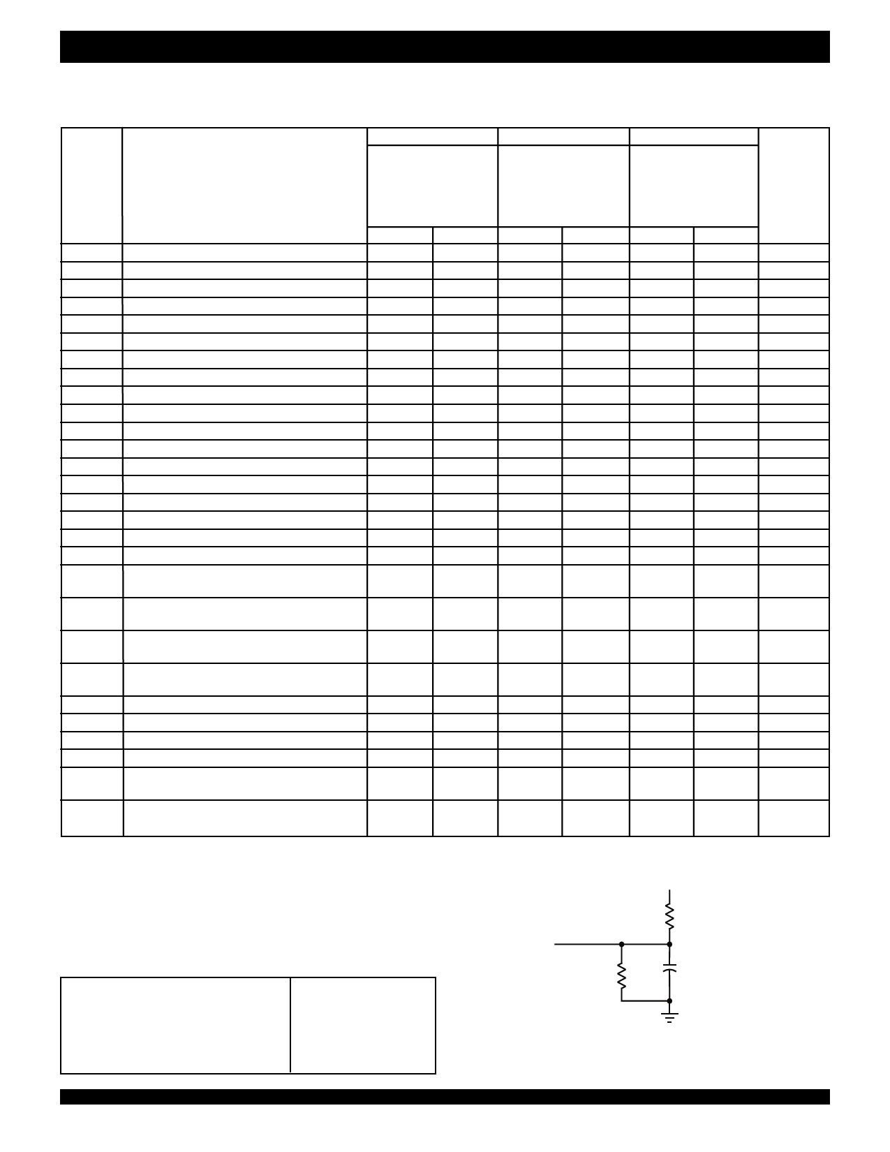
3.3V
330Ω
AC TEST CONDITIONS
Input Pulse Levels
Input Rise/Fall Times
Input Timing Reference Levels
Output Reference Levels
Output Load
GND to 3.0V
3ns
1.5V
1.5V
See Figure 1
5
D.U.T.
510Ω
30pF*
4295 drw 03
Figure 1. Output Load
* Includes jig and scope capacitances.
Share Link: