IDT72V845 View Datasheet(PDF) - Integrated Device Technology
Part Name
Description
View to exact match
IDT72V845
Integrated Device Technology

IDT72V845 Datasheet PDF : 26 Pages
| |||
IDT72V805/72V815/72V825/72V835/72V845
3.3 V CMOS DUAL SyncFIFO™ 256 x 18, 512 x 18, 1,024 x 18, 4,096 x 18
COMMERCIAL AND INDUSTRIAL
TEMPERATURE RANGES
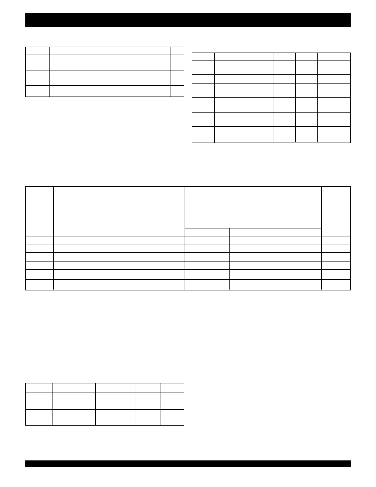
ABSOLUTE MAXIMUM RATINGS
RECOMMENDED OPERATING DC
Symbol
VTERM
TSTG
IOUT
Rating
Terminal Voltage
with respect to GND
Storage
Temperature
DC Output Current
Commercial
–0.5 to +5
–55 to +125
–50 to +50
CONDITIONS
Unit
V
Symbol
Parameter
VCC Supply Voltage
Commercial/Industrial
°C
GND Supply Voltage
mA
VIH
Input High Voltage
Commercial/Industrial
Min. Typ. Max. Unit
3.0
3.3
3.6 V
0
0
0V
2.0
—
5.0 V
VIL(1) Input Low Voltage
NOTE:
Commercial/Industrial
1. Stresses greater than those listed under ABSOLUTE MAXIMUM RATINGS may cause
permanent damage to the device. This is a stress rating only and functional operation TA
Operating Temperature
of the device at these or any other conditions above those indicated in the operational
Commercial
sections of this specification is not implied. Exposure to absolute maximum rating TA
conditions for extended periods may affect reliability.
Operating Temperature
Industrial
—
—
0.8 V
0
—
70 °C
-40
85 °C
NOTE:
1. 1.5V undershoots are allowed for 10ns once per cycle.
DC ELECTRICAL CHARACTERISTICS
(Commercial: VCC = 3.3V ± 0.3V, TA = 0°C to +70°C; Industrial: VCC = 3.3V ± 0.3V, TA = -40°C to +85°C)
Symbol
ILI(2)
ILO(3)
VOH
VOL
Parameter
Input Leakage Current (any input)
Output Leakage Current
Output Logic “1” Voltage, IOH = –2 mA
Output Logic “0” Voltage, IOL = 8 mA
IDT72V805
IDT72V815
IDT72V825
IDT72V835
IDT72V845
Commercial & Industrial(1)
tCLK = 10, 15, 20 ns
Min.
Typ.
Max.
Unit
–1
—
1
µA
–10
—
10
µA
2.4
—
—
V
—
—
0.4
V
ICC1(4,5,6)
Active Power Supply Current
—
—
60
mA
ICC2(4,7)
Standby Current
—
—
10
mA
NOTES:
1. Industrial temperature range product for the 15ns speed grade is available as a standard device.
2. Measurements with 0.4 ≤ VIN ≤ VCC.
3. OE ≥ VIH, 0.4 ≤ VOUT ≤ VCC.
4. Tested with outputs disabled (IOUT = 0).
5. RCLK and WCLK toggle at 20 MHZ and data inputs switch at 10 MHz.
6. Typical ICC1 = 2[2.04 + 0.88*fS + 0.02*CL*fS] (in mA).
These equations are valid under the following conditions:
VCC = 3.3V, TA = 25°C, fS = WCLK frequency = RCLK frequency (in MHz, using TTL levels), data switching at fS/2, CL = capacitive load (in pF).
7. All Inputs = VCC –0.2V or GND + 0.2V, except RCLK and WCLK, which toggle at 20 MHz.
CAPACITANCE
(TA = +25°C, f = 1.0MHz)
Symbol Parameter(1)
Conditions
CIN(2)
COUT(1,2)
Input
Capacitance
Output
Capacitance
VIN = 0V
VOUT = 0V
NOTES:
1. With output deselected, (OE ≥ VIH).
2. Characterized values, not currently tested.
Max.
Unit
10
pF
10
pF
4
Share Link: