ICM-102ASA View Datasheet(PDF) - Unspecified
Part Name
Description
View to exact match
ICM-102ASA Datasheet PDF : 15 Pages
| |||
ICM102A CIF CMOS sensor
Data Sheet Version1.0 July 2002
processing (i.e., color interpolation and color correction) in order to approximate the full visible spectrum.
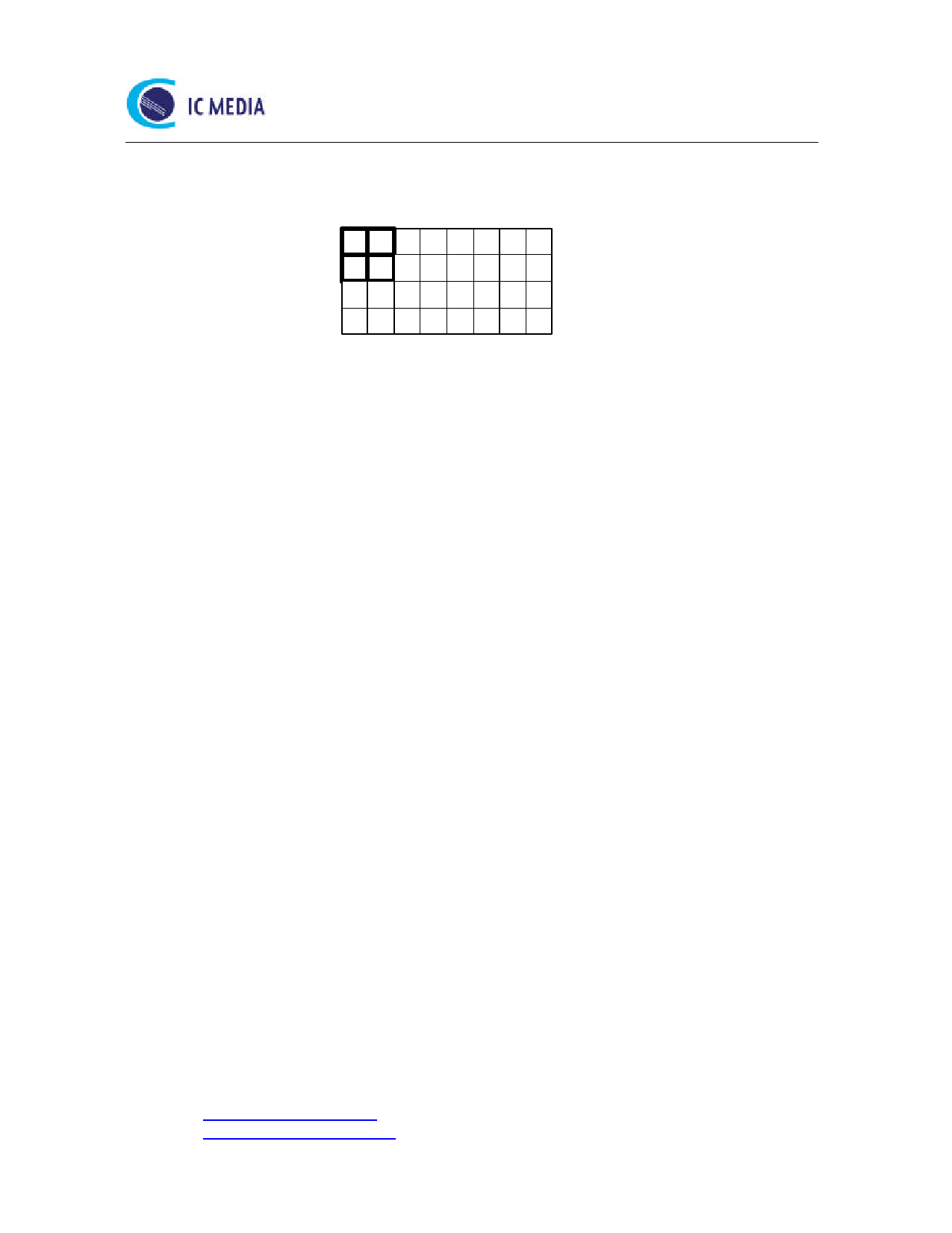
RGRGRGRG
GBGBGBGB
RGRGRGRG
GBGBGBGB
Figure 2. Color filter Bayer pattern
2.3 Exposure and Gain Control
The brightness of the scene may change by a great amount that renders the captured image either
over-exposed or under-exposed. To accommodate for different brightness, the user may change the
exposure time by adjusting the AD_EXPOSE_TIMEH, and AD_EXPOSE_TIMEL. The exposure time is
measured in terms of the time to read out one line of data, which is equal to 83.3 µs (assuming the line
length is 500 @ 12 MHz). If the number of lines per frame is set at 400 (the default), the exposure time can
vary from 1 to 399 lines. In addition, users can adjust bit 7 to 5 of register AD_COL_BEGINH to digitally
boost the output value by 1 to 64 times @ 2N for all the pixels. Furthermore, users can adjust registers
AD_M1_L, AD_M1_H, AD_M2_L, AD_M2_H, AD_M3_L, AD_M3_H, AD_M4_L, AD_M4_H, to
optimize the individual R/G1/G2/B gain (default at 3.8 format for 1/256 to 8) of the 4 Bayer pattern
pixels separately.
2.4 Output Format
During normal operation, the output format is 8-bit raw data that ranges from 0 to 255. It may be used for
off-chip color processing or compression. A typical configuration is to connect ICM-102A to a
USB/Compression combo chip. When operated at 30 fps, the PCLK is 6 MHz when the input main clock
is 12 MHz.
In addition to the data pins, the chip also output VSYNC, HSYNC, BLANK, and PCLK. The length and
polarity of VSYNC and HSYNC can be adjusted through registers. The line and frame timing can be
adjusted through registers AD_WIDTH and AD_HEIGHT.
2.5 SIF Interface
Register programming is through SIF interface (SCL and SDA pins). The 7-bit SIF device address is 0x20
by default, but the last bit can be configured by the SIFID pin. ICM-102A can operate in either SIF master
mode or slave mode right after power up, depending on the pull-up or pull-down of the MSSEL pin.
When MSSEL is pulled low during power-up, ICM-102A’s SIF interface is operated as an SIF slave device,
waiting to be controlled by an external SIF master such as a microprocessor. When MSSEL is pulled high
during power-up, the SIF interface is first acting as an SIF master device trying to read from an external
SIF EEPROM. After that, it will fall back to behave like an SIF slave.
3. SIF Registers
©2000, 2001, 2002 IC Media Corporation & IC Media Technology Corp.
web site: http://www.ic- media.com/
web site: http://www.ic- media.com.tw/
page 7
7/24/2002
Share Link: 