MC74HC195N View Datasheet(PDF) - Motorola => Freescale
Part Name
Description
View to exact match
MC74HC195N Datasheet PDF : 7 Pages
| |||
MC74HC195
PIN DESCRIPTION
DATA INPUTS
A, B, C, D (Pins 4, 5, 6, 7)
Parallel data inputs.
OUTPUTS
QA, QB, QC, QD, QD (Pins 15, 14, 13, 12, 11)
Parallel data outputs.
CONTROL INPUTS
Clock (Pin 10)
Clock input. The shift register is completely static, allowing
Clock rates down to DC in a continuous or intermittent mode.
Serial Shift/Parallel Load (Pin 9)
Shift or load control. A low level applied to this pin allows
data to be loaded from the parallel inputs. Data is loaded with
the positive transition of the Clock input. A high level allows
data to be shifted in the manner dictated by the J and K con-
trol inputs.
Reset (Pin 1)
A low level applied to this pin resets all stages and forces
all outputs low.
J, K (Pins 2, 3)
Shift Control. With Serial Shift/Parallel Load high, J and K
control the mode of operation, as illustrated in the Function
Table.
J = L, K = H
With a positive transition of the Clock input, each bit is
shifted to the right (in the direction QA toward QD) one stage
and stage A maintains its previous state.
J = H, K = L
With a positive transition of the Clock input, each bit is
shifted right (in the direction of QA toward QD) one stage and
the QA output is inverted.
J=K=L
With a positive transition of the Clock input, each bit is
shifted right (in the direction QA toward QD) one stage and a
low is loaded into stage A.
J=K=H
With a positive transition of the Clock input, each bit is
shifted right (in the direction QA toward QD) one stage and a
high is loaded into stage A.
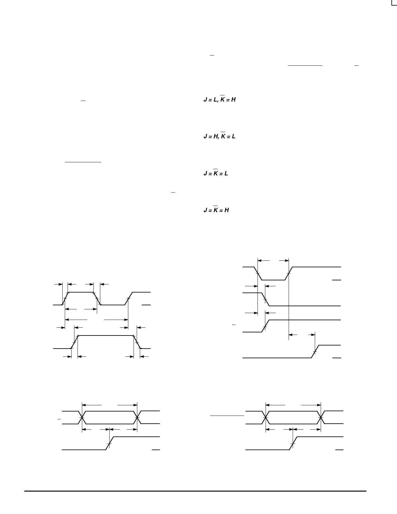
SWITCHING WAVEFORMS
tr
tf
CLOCK
90%
50%
VCC
10%
GND
tw
90%
Q 50%
10%
1/fmax
tPLH
tPHL
tTLH
tTHL
Figure 1.
tw
VCC
RESET
50%
GND
tPHL
Q
50%
tPLH
Q
50%
trec
CLOCK
VCC
50%
GND
Figure 2.
INPUT
A, B, C,
D, J, OR K
CLOCK
VALID
50%
tsu
th
50%
Figure 3.
MOTOROLA
VALID
VCC
SERIAL SHIFT
VCC
GND
PARALLEL LOAD
50%
GND
tsu
th
VCC
VCC
CLOCK
50%
GND
GND
Figure 4.
3–4
High–Speed CMOS Logic Data
DL129 — Rev 6
Share Link: 