M27C4001-35B1TR View Datasheet(PDF) - STMicroelectronics
Part Name
Description
View to exact match
M27C4001-35B1TR Datasheet PDF : 17 Pages
| |||
M27C4001
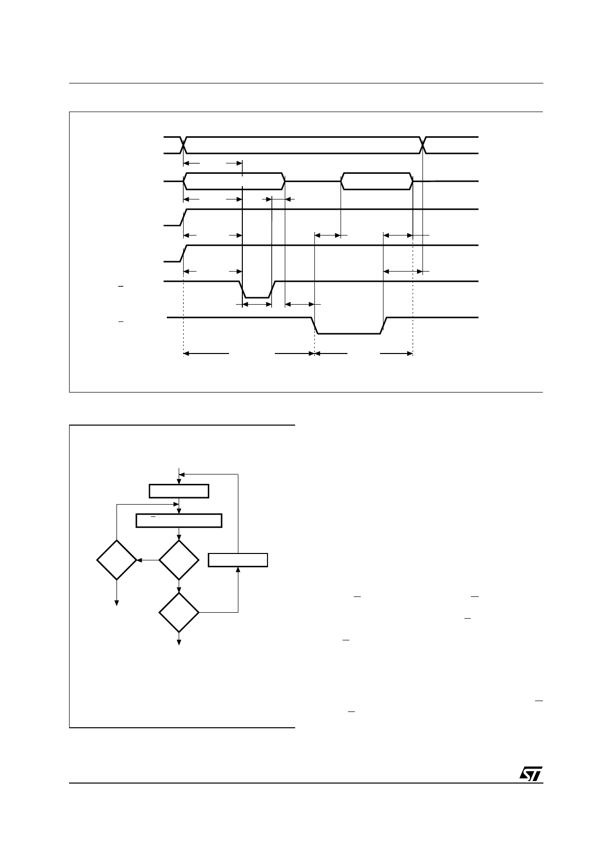
Figure 6. Programming and Verify Modes AC Waveforms
A0-A18
Q0-Q7
VPP
VCC
E
G
tAVPL
DATA IN
tQVEL
tVPHEL
tVCHEL
tELEH
VALID
tEHQX
DATA OUT
tGLQV
tQXGL
PROGRAM
VERIFY
tGHQZ
tGHAX
AI00725
Figure 7. Programming Flowchart
VCC = 6.25V, VPP = 12.75V
n=0
NO
++n
= 25
YES
E = 100µs Pulse
NO
VERIFY
YES
++ Addr
FAIL
Last NO
Addr
YES
CHECK ALL BYTES
1st: VCC = 6V
2nd: VCC = 4.2V
AI00760B
PRESTO II Programming Algorithm
PRESTO II Programming Algorithm allows the
whole array to be programmed with a guaranteed
margin, in a typical time of 52.5 seconds. Pro-
gramming with PRESTO II consists of applying a
sequence of 100µs program pulses to each byte
until a correct verify occurs (see Figure 7). During
programming and verify operation, a MARGIN
MODE circuit is automatically activated in order to
guarantee that each cell is programmed with
enough margin. No overprogram pulse is applied
since the verify in MARGIN MODE provides the
necessary margin to each programmed cell.
Program Inhibit
Programming of multiple M27C4001s in parallel
with different data is also easily accomplished. Ex-
cept for E, all like inputs including G of the parallel
M27C4001 may be common. A TTL low level
pulse applied to a M27C4001’s E input, with VPP
at 12.75V, will program that M27C4001. A high
level E input inhibits the other M27C4001s from
being programmed.
Program Verify
A verify (read) should be performed on the pro-
grammed bits to determine that they were correct-
ly programmed. The verify is accomplished with G
at VIL, E at VIH, VPP at 12.75V and VCC at 6.25V.
8/17
Share Link: 