M27C4001-35B1TR View Datasheet(PDF) - STMicroelectronics
Part Name
Description
View to exact match
M27C4001-35B1TR Datasheet PDF : 17 Pages
| |||
M27C4001
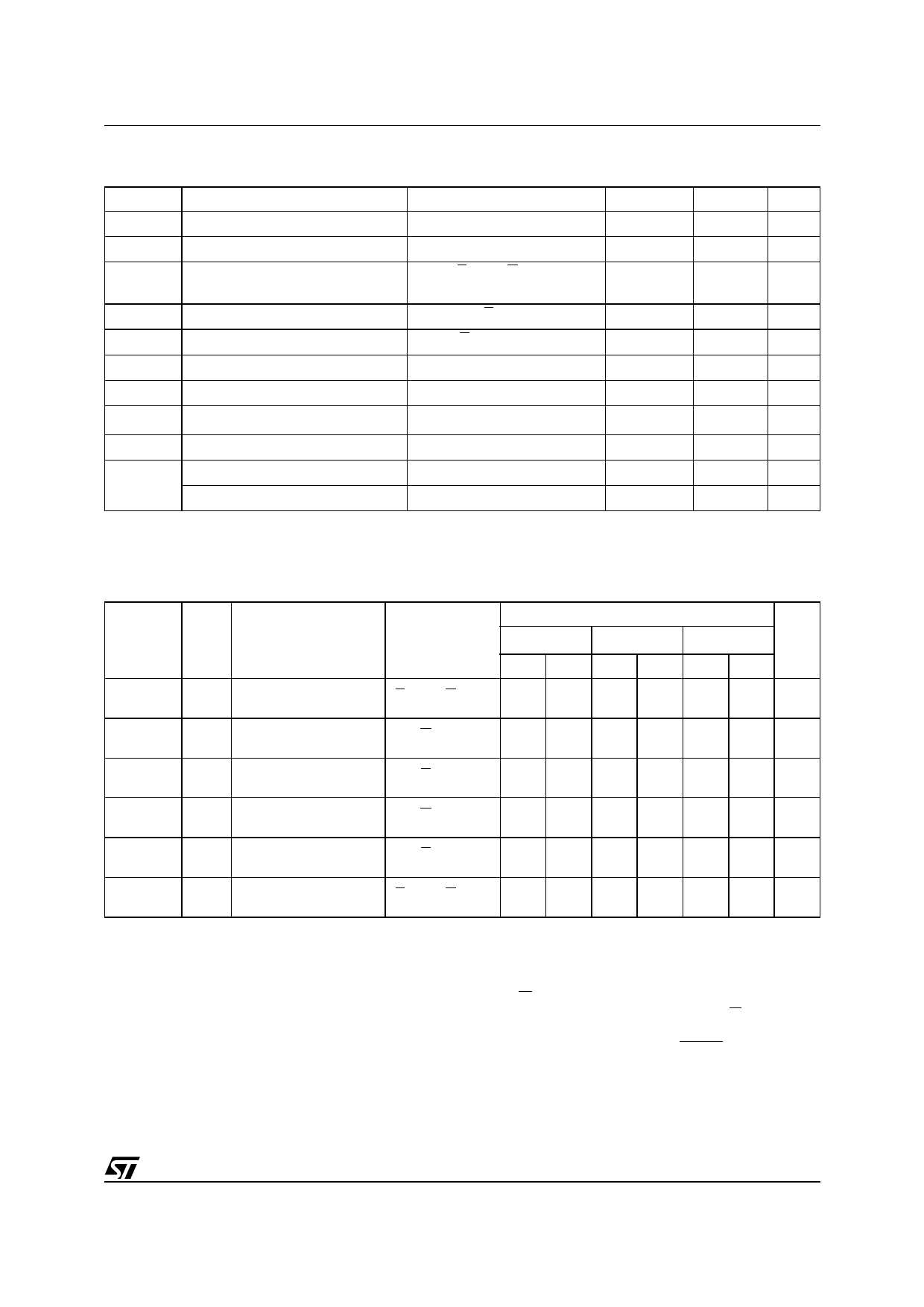
Table 7. Read Mode DC Characteristics (1)
(TA = 0 to 70 °C or –40 to 85 °C; VCC = 5V ± 5% or 5V ± 10%; VPP = VCC)
Symbol
Parameter
Test Condition
Min
ILI
Input Leakage Current
0V ≤ VIN ≤ VCC
ILO
Output Leakage Current
0V ≤ VOUT ≤ VCC
ICC
Supply Current
E = VIL, G = VIL,
IOUT = 0mA, f = 5MHz
ICC1 Supply Current (Standby) TTL
E = VIH
ICC2 Supply Current (Standby) CMOS
E > VCC – 0.2V
IPP
Program Current
VPP = VCC
VIL
Input Low Voltage
–0.3
VIH (2) Input High Voltage
2
VOL Output Low Voltage
IOL = 2.1mA
Output High Voltage TTL
VOH
Output High Voltage CMOS
IOH = –400µA
IOH = –100µA
2.4
VCC – 0.7V
Note: 1. VCC must be applied simultaneously with or before VPP and removed simultaneously or after VPP.
2. Maximum DC voltage on Output is VCC +0.5V.
Max
±10
±10
30
1
100
10
0.8
VCC + 1
0.4
Unit
µA
µA
mA
mA
µA
µA
V
V
V
V
V
Table 8A. Read Mode AC Characteristics (1)
(TA = 0 to 70 °C or –40 to 85 °C; VCC = 5V ± 5% or 5V ± 10%; VPP = VCC)
M27C4001
Symbol Alt
Parameter
Test Condition
-35 (3)
-45 (3)
Min Max Min Max
tAVQV
tACC
Address Valid to
Output Valid
E = VIL, G = VIL
35
45
tELQV
tCE
Chip Enable Low to
Output Valid
G = VIL
35
45
tGLQV
tOE
Output Enable Low to
Output Valid
E = VIL
20
25
tEHQZ (2)
tDF
Chip Enable High to
Output Hi-Z
G = VIL
0
30
0
30
tGHQZ (2)
tDF
Output Enable High to
Output Hi-Z
E = VIL
0
30
0
30
tAXQX
tOH
Address Transition to
Output Transition
E = VIL, G = VIL 0
0
-55 (3)
Min Max
55
55
30
0
30
0
30
0
Unit
ns
ns
ns
ns
ns
ns
Note: 1. VCC must be applied simultaneously with or before VPP and removed simultaneously or after VPP
2. Sampled only, not 100% tested.
3. Speed obtained with High Speed AC measurement conditions.
Two Line Output Control
Because EPROMs are usually used in larger
memory arrays, this product features a 2 line con-
trol function which accommodates the use of mul-
tiple memory connection. The two line control
function allows:
a. the lowest possible memory power dissipation,
b. complete assurance that output bus contention
will not occur.
For the most efficient use of these two control
lines, E should be decoded and used as the prima-
ry device selecting function, while G should be
made a common connection to all devices in the
array and connected to the READ line from the
system control bus. This ensures that all deselect-
ed memory devices are in their low power standby
mode and that the output pins are only active
when data is required from a particular memory
device.
5/17
Share Link: 