CY7C4205V View Datasheet(PDF) - Cypress Semiconductor
Part Name
Description
View to exact match
CY7C4205V Datasheet PDF : 20 Pages
| |||
CY7C4225V/4205V/4215V
CY7C4425V/4235V/4245V
Switching Characteristics Over the Operating Range (continued)
Parameter
tXO
tXI
tXIS
tSKEW1
tSKEW2
tSKEW3
Description
Clock to Expansion Out
Expansion in Pulse Width
Expansion in Set-up Time
Skew Time between Read Clock and Write Clock for
Full Flag
Skew Time between Read Clock and Write Clock for
Empty Flag
Skew Time between Read Clock and Write Clock for
Programmable Almost Empty and Programmable
Almost Full Flags.
7C42X5V-15 7C42X5V-25 7C42X5V-35
Min. Max. Min. Max. Min. Max. Unit
10
15
20 ns
6.5
10
14
ns
5
10
15
ns
6
10
12
ns
6
10
12
ns
15
18
20
ns
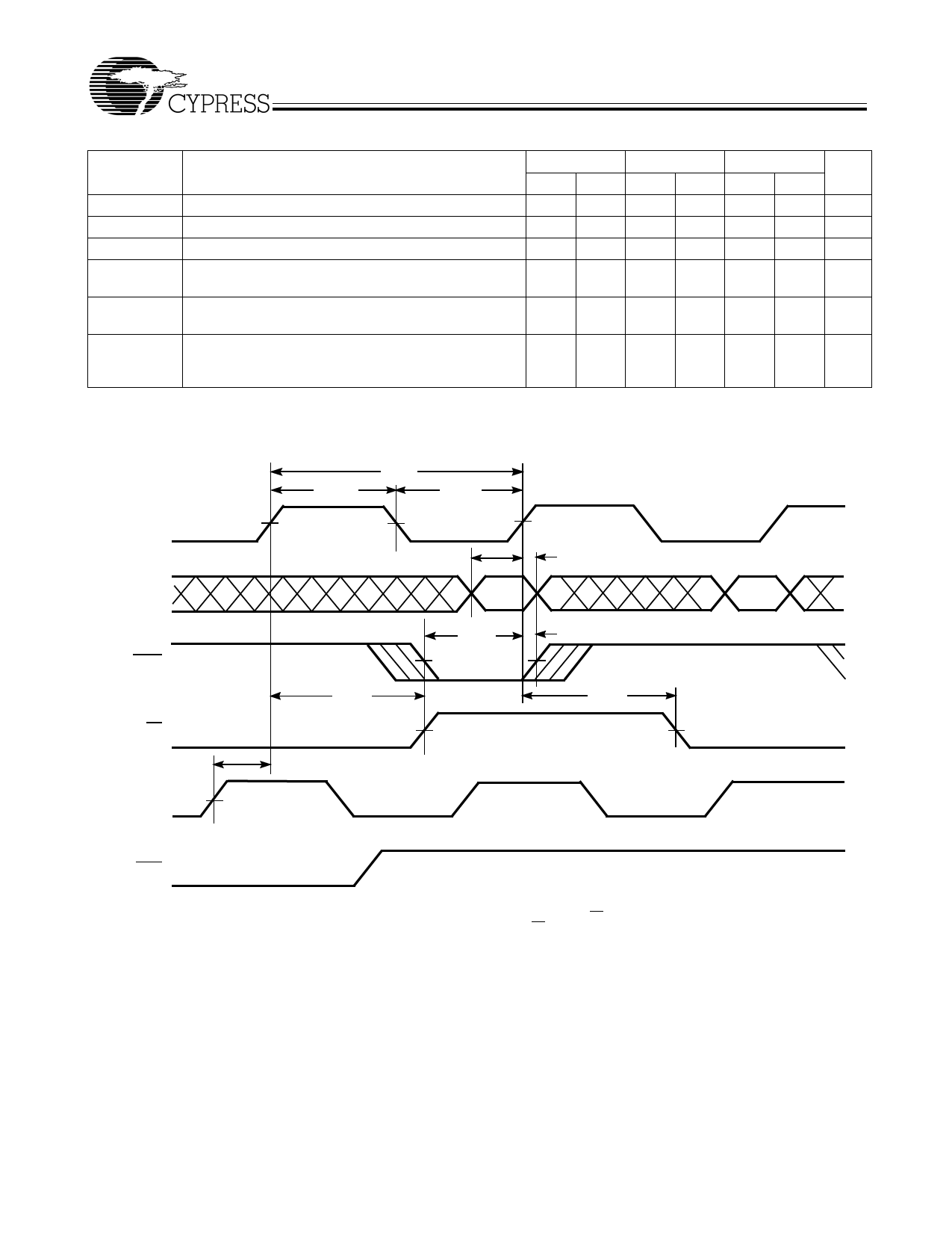
Switching Waveforms
Write Cycle Timing
tCLKH
tCLK
tCLKL
WCLK
D0–D17
WEN
tWFF
tDS
tENS
tDH
tENH
tWFF
NO OPERATION
FF
RCLK
tSKEW1[14]
REN
Note:
14. tSKEW1 is the minimum time between a rising RCLK edge and a rising WCLK edge to guarantee that FF will go HIGH during the current clock cycle. If the time
between the rising edge of RCLK and the rising edge of WCLK is less than tSKEW1, then FF may not change state until the next WCLK edge.
Document #: 38-06029 Rev. *C
Page 10 of 20
Share Link: 