CY7C4205V View Datasheet(PDF) - Cypress Semiconductor
Part Name
Description
View to exact match
CY7C4205V Datasheet PDF : 20 Pages
| |||
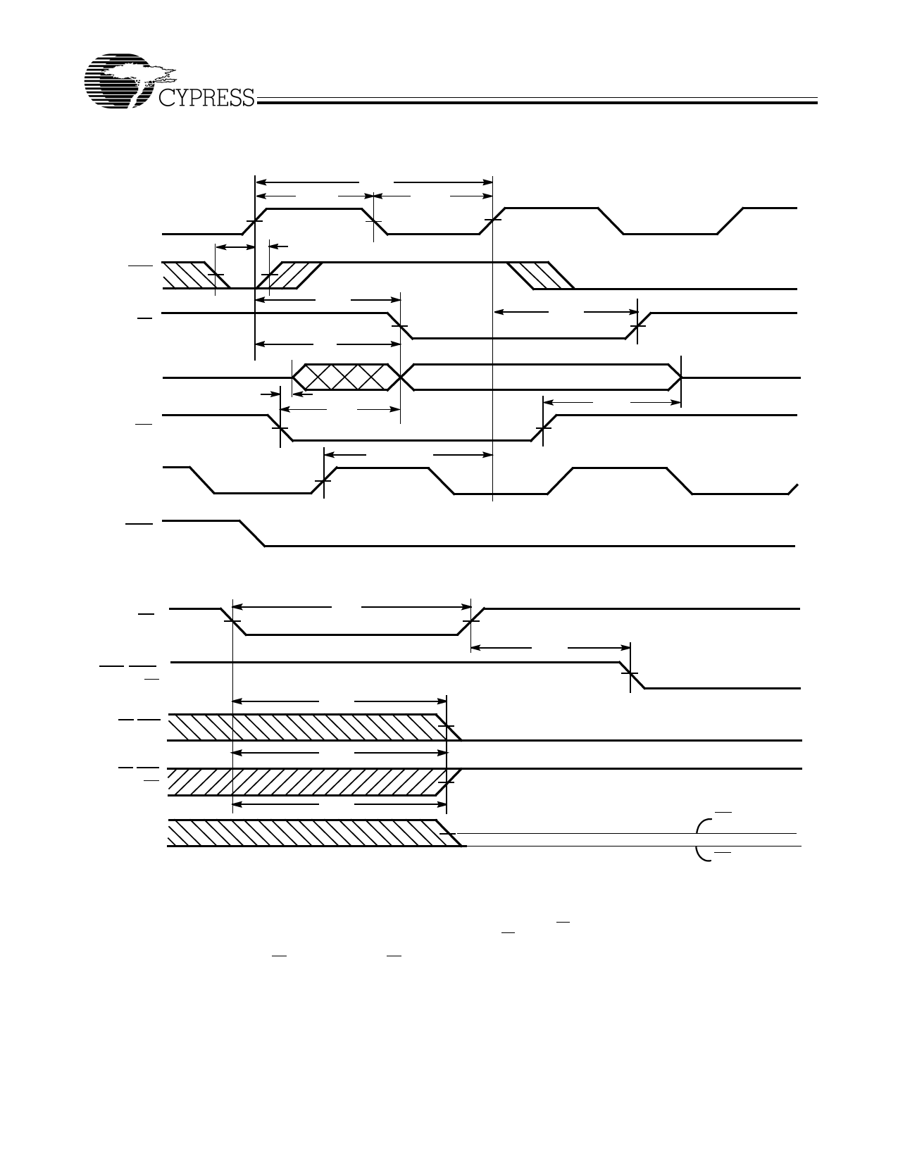
Switching Waveforms (continued)
Read Cycle Timing
RCLK
REN
tENS
EF
tCLKH
tCLK
tCLKL
tENH
tREF
tA
NO OPERATION
Q0–Q17
OE
WCLK
tOLZ
tOE
tSKEW2[15]
WEN
Reset Timing[16]
tRS
RS
REN, WEN,
LD
EF,PAE
FF,PAF,
HF
Q0–Q17
tRSF
tRSF
tRSF
CY7C4225V/4205V/4215V
CY7C4425V/4235V/4245V
tREF
VALID DATA
tOHZ
tRSR
OE = [117]
OE = 0
Notes:
15. tSKEW2 is the minimum time between a rising WCLK edge and a rising RCLK edge to guarantee that EF will go HIGH during the current clock cycle. It the time
between the rising edge of WCLK and the rising edge of RCLK is less than tSKEW2, then EF may not change state until the next RCLK edge.
16. The clocks (RCLK, WCLK) can be free-running during reset.
17. After reset, the outputs will be LOW if OE = 0 and three-state if OE = 1.
Document #: 38-06029 Rev. *C
Page 11 of 20
Share Link: 