AT27BV1024-90JC View Datasheet(PDF) - Atmel Corporation
Part Name
Description
View to exact match
AT27BV1024-90JC
Atmel Corporation

AT27BV1024-90JC Datasheet PDF : 9 Pages
| |||
AT27BV1024
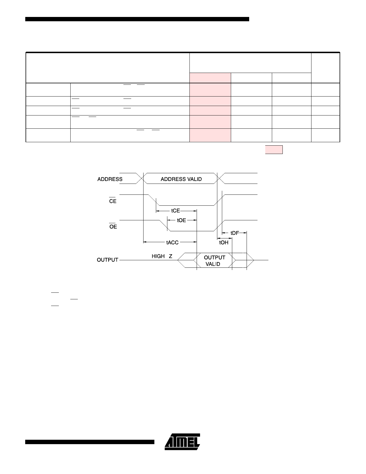
AC Characteristics for Read Operation (VCC = 2.7V to 3.6V and 4.5V to 5.5V)
AT27BV1024
-90
-12
-15
Symbol
Parameter
Condition
tACC (3)
tCE (2)
tOE (2, 3)
tDF (4, 5)
tOH
Address to
Output Delay
CE = OE
= VIL
CE to Output Delay OE = VIL
OE to Output Delay CE = VIL
OE or CE High to Output Float,
whichever occurred first
Output Hold from Address, CE or OE,
whichever occurred first
Notes: 2, 3, 4, 5. - see AC Waveforms for Read Operation.
Min Max Min Max Min Max
Units
90
120
150
ns
90
120
150
ns
30
35
50
ns
30
30
40
ns
0
0
0
ns
= Preliminary Information
AC Waveforms for Read Operation (1)
Notes: 1. Timing measurement references are 0.8V and 2.0V.
Input AC drive levels are 0.45V and 2.4V, unless oth-
erwise specified.
2. OE may be delayed up to tCE - tOE after the falling
edge of CE without impact on tCE.
3. OE may be delayed up to tACC - tOE after the address
is valid without impact on tACC.
4. This parameter is only sampled and is not 100% tested.
5. Output float is defined as the point when data is no longer
driven.
6. When reading a 27BV1024, a 0.1 µF capacitor is required
across VCC and ground to supress spurious voltage tran-
sients.
3-37
Share Link: