AT27BV1024-90JC View Datasheet(PDF) - Atmel Corporation
Part Name
Description
View to exact match
AT27BV1024-90JC
Atmel Corporation

AT27BV1024-90JC Datasheet PDF : 9 Pages
| |||
AT27BV1024
Features
Fast Read Access Time - 90 ns
•• Dual Voltage Range Operation
Unregulated Battery Power Supply Range, 2.7V to 3.6V
or Standard 5V ± 10% Supply Range
Pin Compatible with JEDEC Standard AT27C1024
•• Low Power CMOS Operation
20 µA max. (less than 1 µA typical) Standby for VCC = 3.6V
29 mW max. Active at 5 MHz for VCC = 3.6V
• JEDEC Standard Surface Mount Packages
44-Lead PLCC
40-Lead TSOP (10 x 14mm)
• High Reliability CMOS Technology
2,000V ESD Protection
200 mA Latchup Immunity
• Rapid™ Programming Algorithm - 100 µs/word (typical)
• CMOS and TTL Compatible Inputs and Outputs
JEDEC Standard for LVTTL and LVBO
Integrated Product Identification Code
•• Commercial and Industrial Temperature Ranges
Description
The AT27BV1024 is a high performance, low power, low voltage 1,048,576 bit one-
time programmable read only memory (OTP EPROM) organized as 64K by 16 bits.
It requires only one supply in the range of 2.7V to 3.6V in normal read mode opera-
tion. The by-16 organization makes this part ideal for portable and handheld 16 and
32 bit microprocessor based systems using either regulated or unregulated battery
power.
(continued)
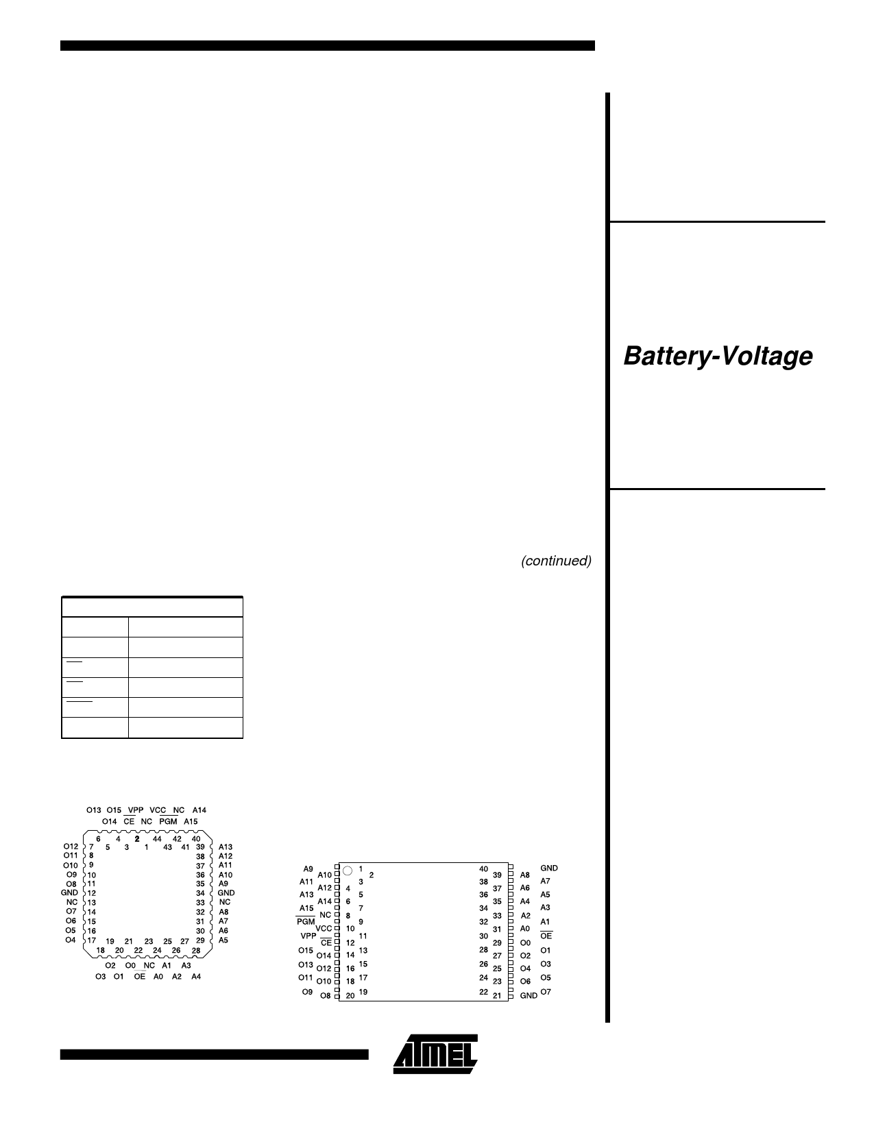
Pin Configurations
Pin Name Function
A0 - A15 Addresses
O0 - O15 Outputs
CE
Chip Enable
OE
Output Enable
PGM
Program Strobe
NC
No Connect
Note: Both GND pins must be
connected.
PLCC Top View
1 Megabit
(64K x 16)
Unregulated
Battery-Voltage™
High Speed
OTP
CMOS EPROM
AT27BV1024
TSOP Top View
Type 1
Note: PLCC Package Pins 1 and
23 are DON’T CONNECT.
0631A
3-33
Share Link: