74LS195 View Datasheet(PDF) - Motorola => Freescale
Part Name
Description
View to exact match
74LS195 Datasheet PDF : 6 Pages
| |||
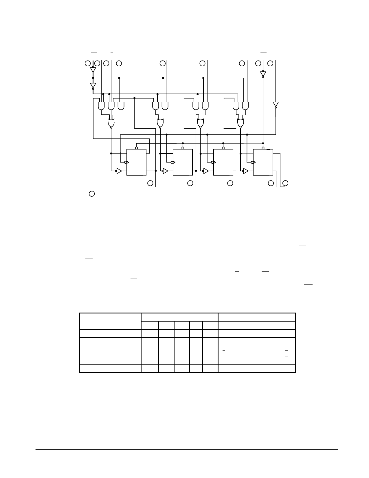
LOGIC DIAGRAM
PE J K P0
923
4
SN54 / 74LS195A
P1
5
P2
6
P3
7
MR CP
1
10
R CD Q0
CP
S Q0
VCC = PIN 16
GND = PIN 8
= PIN NUMBERS
15
Q0
R CD
CP
S Q0
14
Q1
R CD
CP
S Q2
13
Q2
R CD Q3
CP
S Q3
12
11
Q3 Q3
FUNCTIONAL DESCRIPTION
The Logic Diagram and Truth Table indicate the functional
characteristics of the LS195A 4-Bit Shift Register. The device
is useful in a wide variety of shifting, counting and storage
applications. It performs serial, parallel, serial to parallel, or
parallel to serial data transfers at very high speeds.
The LS195A has two primary modes of operation, shift right
(Q0 Q1) and parallel load which are controlled by the state of
the Parallel Enable (PE) input. When the PE input is HIGH,
serial data enters the first flip-flop Q0 via the J and K inputs and
is shifted one bit in the direction Q0 Q1 Q2 Q3 following
each LOW to HIGH clock transition. The JK inputs provide the
flexibility of the JK type input for special applications, and the
simple D type input for general applications by tying the two
pins together. When the PE input is LOW, the LS195A appears
as four common clocked D flip-flops. The data on the parallel
inputs P0, P1, P2, P3 is transferred to the respective Q0, Q1,
Q2, Q3 outputs following the LOW to HIGH clock transition.
Shift left operations (Q3 Q2) can be achieved by tying the Qn
Outputs to the Pn–1 inputs and holding the PE input LOW.
All serial and parallel data transfers are synchronous,
occurring after each LOW to HIGH clock transition. Since the
LS195A utilizes edge-triggering, there is no restriction on the
activity of the J, K, Pn and PE inputs for logic operation —
except for the set-up and release time requirements.
A LOW on the asynchronous Master Reset (MR) input sets
all Q outputs LOW, independent of any other input condition.
MODE SELECT — TRUTH TABLE
OPERATING MODES
Asynchronous Reset
INPUTS
OUTPUTS
MR PE J K Pn Q0 Q1 Q2 Q3 Q3
L
X
XXX
L
L
L
LH
Shift, Set First Stage
H
h
h
h
X
H q0 q1 q2 q2
Shift, Reset First
H
h
I
IX
L q0 q1 q2 q2
Shift, Toggle First Stage
H
h
h
I
X q0 q0 q1 q2 q2
Shift, Retain First Stage
H
h
I
h
X q0 q0 q1 q2 q2
Parallel Load
H
I
X X pn p0 p1 p2 p3 p3
L = LOW voltage levels
H = HIGH voltage levels
X = Don’t Care
I = LOW voltage level one set-up time prior to the LOW to HIGH clock transition.
h = HIGH voltage level one set-up time prior to the LOW to HIGH clock transition.
pn (qn) = Lower case letters indicate the state of the referenced input (or output) one set-up time prior to the LOW to
HIGH clock transition.
FAST AND LS TTL DATA
5-367
Share Link: 