AT27BV1024 View Datasheet(PDF) - Atmel Corporation
Part Name
Description
View to exact match
AT27BV1024 Datasheet PDF : 14 Pages
| |||
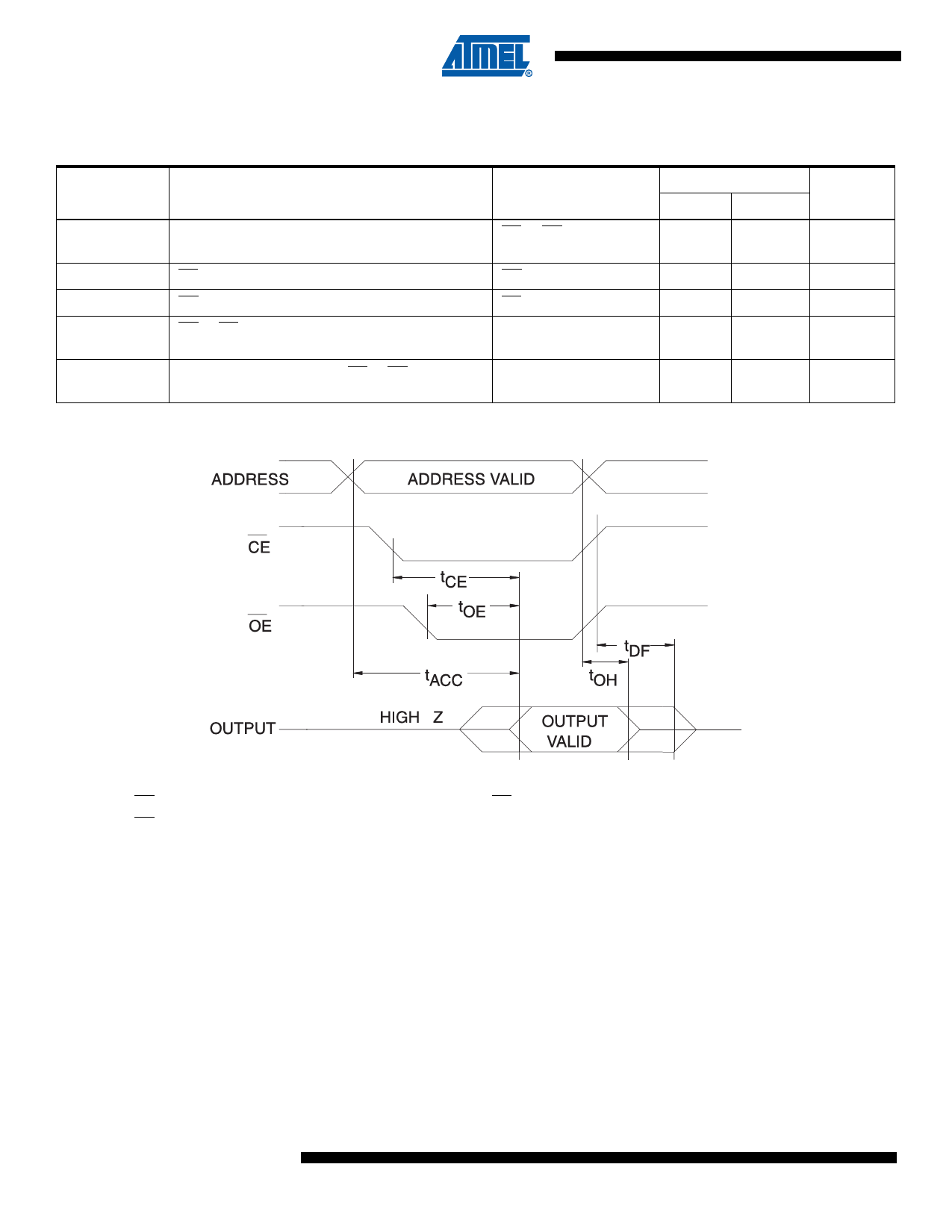
9. AC Characteristics for Read Operation
VCC = 2.7V to 3.6V and 4.5V to 5.5V
Symbol
tACC(3)
tCE(2)
tOE(2)(3)
tDF(4)(5)
tOH
Parameter
Address to Output Delay
CE to Output Delay
OE to Output Delay
OE or CE High to Output Float, Whichever
Occurred First
Output Hold from Address, CE or OE,
Whichever Occurred First
10. AC Waveforms for Read Operation(1)
Condition
CE = OE
= VIL
OE = VIL
CE = VIL
AT27BV1024-90
Min
Max
Unit
90
ns
90
ns
30
ns
30
ns
0
ns
Notes:
1. Timing measurement references are 0.8V and 2.0V. Input AC drive levels are 0.45V and 2.4V, unless otherwise specified.
2. OE may be delayed up to tCE - tOE after the falling edge of CE without impact on tCE.
3. OE may be delayed up to tACC - tOE after the address is valid without impact on tACC.
4. This parameter is only sampled and is not 100% tested.
5. Output float is defined as the point when data is no longer driven.
6. When reading a AT27BV1024, a 0.1 µF capacitor is required across VCC and ground to suppress spurious voltage
transients.
6 AT27BV1024
0631E–EPROM–12/07
Share Link: 