SST89V516RD2-33-C-TQJE View Datasheet(PDF) - Microchip Technology
Part Name
Description
View to exact match
SST89V516RD2-33-C-TQJE Datasheet PDF : 94 Pages
| |||
FlashFlex MCU
SST89E516RD2 / SST89E516RD
SST89V516RD2 / SST89V516RD
Pin Descriptions
Data Sheet
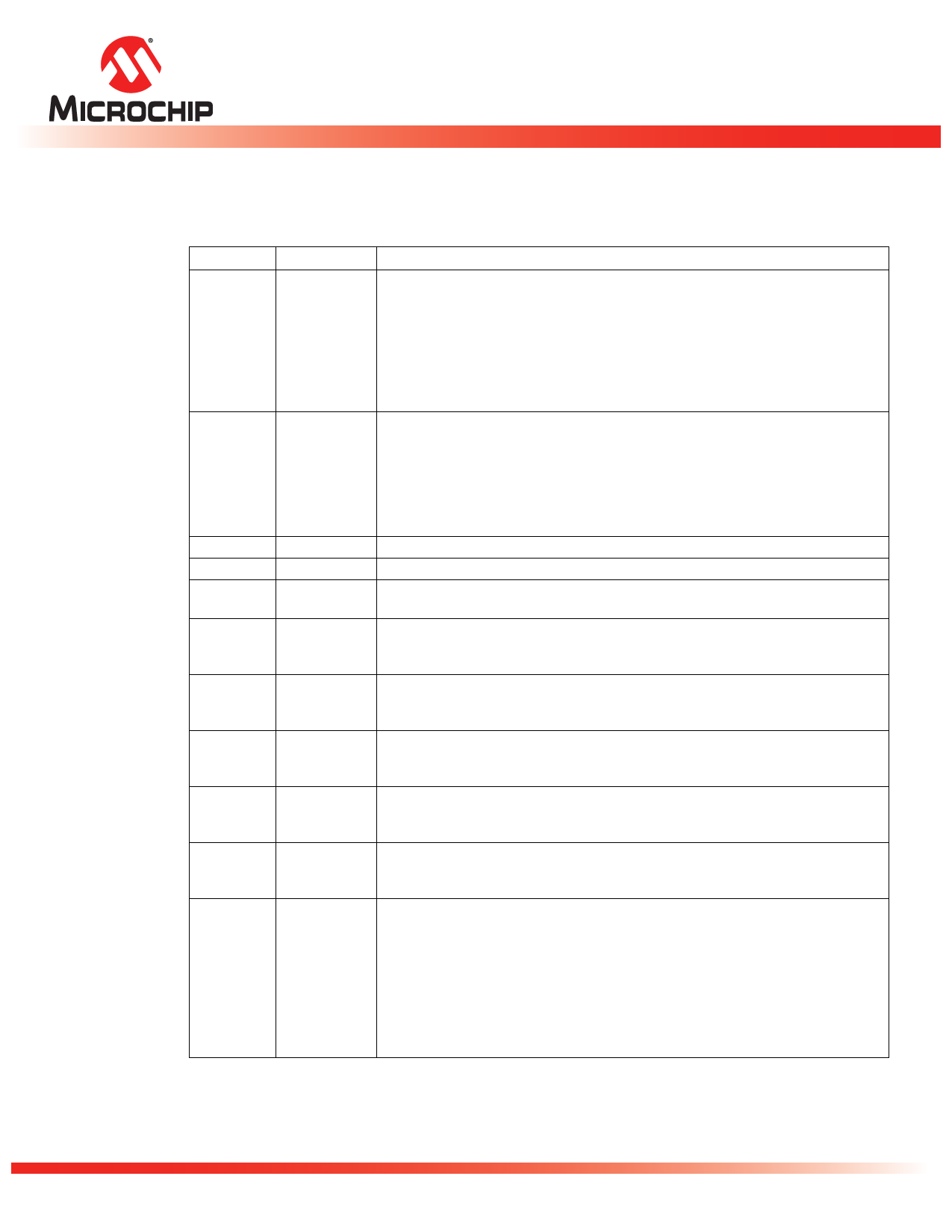
Table 1: Pin Descriptions (1 of 3)
Symbol
Type1
Name and Functions
P0[7:0]
I/O
Port 0: Port 0 is an 8-bit open drain bi-directional I/O port. As an output port each
pin can sink several LS TTL inputs. Port 0 pins float that have ‘1’s written to them,
and in this state can be used as high-impedance inputs. Port 0 is also the multi-
plexed low-order address and data bus during accesses to external memory. In
this application, it uses strong internal pull-ups when transitioning to VOH. Port 0
also receives the code bytes during the external host mode programming, and
outputs the code bytes during the external host mode verification. External pull-
ups are required during program verification.
P1[7:0]
I/O with inter-
nal pull-ups
Port 1: Port 1 is an 8-bit bi-directional I/O port with internal pull-ups. The Port 1
output buffers can drive LS TTL inputs. Port 1 pins are pulled high by the internal
pull-ups when “1”s are written to them and can be used as inputs in this state. As
inputs, Port 1 pins that are externally pulled low will source current because of the
internal pull-ups. P1[5, 6, 7] have high current drive of 16 mA. Port 1 also receives
the low-order address bytes during the external host mode programming and ver-
ification.
P1[0]
I/O
T2: External count input to Timer/Counter 2 or Clock-out from Timer/Counter 2
P1[1]
I
T2EX: Timer/Counter 2 capture/reload trigger and direction control
P1[2]
I
ECI: PCA Timer/Counter External Input:
This signal is the external clock input for the PCA timer/counter.
P1[3]
I/O
CEX0: Compare/Capture Module External I/O
Each compare/capture module connects to a Port 1 pin for external I/O. When not
used by the PCA, this pin can handle standard I/O.
P1[4]
I/O
SS#: Master Input or Slave Output for SPI.
OR
CEX1: Compare/Capture Module External I/O
P1[5]
I/O
MOSI: Master Output line, Slave Input line for SPI
OR
CEX2: Compare/Capture Module External I/O
P1[6]
I/O
MISO: Master Input line, Slave Output line for SPI
OR
CEX3: Compare/Capture Module External I/O
P1[7]
I/O
SCK: Master clock output, slave clock input line for SPI
OR
CEX4: Compare/Capture Module External I/O
P2[7:0]
I/O with inter-
nal pull-up
Port 2: Port 2 is an 8-bit bi-directional I/O port with internal pull-ups. Port 2 pins
are pulled high by the internal pull-ups when “1”s are written to them and can be
used as inputs in this state. As inputs, Port 2 pins that are externally pulled low will
source current because of the internal pull-ups. Port 2 sends the high-order
address byte during fetches from external Program memory and during accesses
to external Data Memory that use 16-bit address (MOVX@DPTR). In this applica-
tion, it uses strong internal pull-ups when transitioning to VOH. Port 2 also receives
some control signals and high-order address bits during the external host mode
programming and verification.
©2013 Silicon Storage Technology, Inc.
8
DS25093B
02/13
Share Link: 