MSK621 View Datasheet(PDF) - M.S. Kennedy
Part Name
Description
View to exact match
MSK621 Datasheet PDF : 6 Pages
| |||
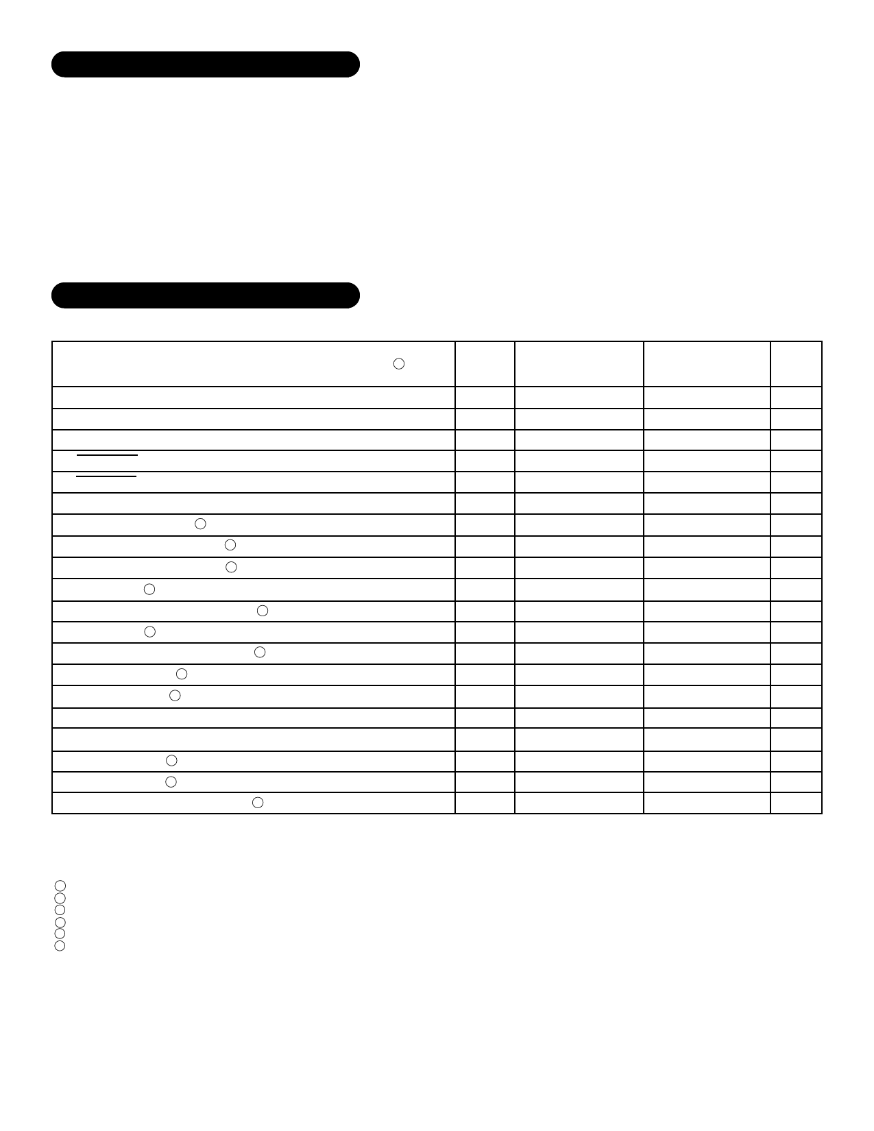
ABSOLUTE MAXIMUM RATINGS
+VCC
-VEE
θJC
VIN
IOUT
IOUTREF
Supply Voltage ○ ○ ○ ○ ○ ○ ○ ○ ○ ○ ○ ○ ○ +13.5V TST
Supply Voltage -8V T ○
○
○
○
○
○
○
○
○
○
○
○
○
○
○
○
LD
Thermal Resistance ○ ○ ○ ○ ○ ○ ○ ○ ○ 19.0°C/W
(Junction to Case)
TC
Voltage At Any Input Pin○ ○ ○ ○Vcc≥Vin≥GND
Video Output Current ○ ○ ○ ○ ○ ○ ○ ○ ○ ○ 100mA
Reference Output Current ○ ○ ○ ○ ○ ○ ○ ○ 20mA TJ
Storage Temperature Range -65°C to +150°C
Lead Temperature Range○ ○ ○ ○ ○ ○ ○ ○ ○ ○ 300°C
(10 Seconds)
Case Operating Temperature
MSK621 ○ ○ ○ ○ ○ ○ ○ ○ ○ ○ ○ ○ -40°C to +85°C
MSK621B ○ ○ ○ ○ ○ ○ ○ ○ ○ ○ ○ -55°C to +125°C
Junction Temperature ○ ○ ○ ○ ○ ○ ○ ○ ○ ○ ○ ○ 150°C
ELECTRICAL SPECIFICATIONS
+Vcc=+12.0V, -VEE=-5V Unless Otherwise Specified
Parameter
Test Conditions 1
STATIC
Power Supply Current
RLOAD=∞; +VCC
Video Input Bias Voltage
VIN=N/C
Clamp Gate High Input Voltage
Comparator Off
Clamp Gate Low Input Voltage
Comparator On
DYNAMIC CHARACTERISTICS
Video Amplifier Gain 5
Video Output Low Voltage 5
Clamp Cap Voltage = 0V
Video Output High Voltage 5
Clamp Cap Voltage = 6V
Attenuation 2
VCONTRAST=0.5V
Video Amplifier Input Resistance 2
fIN=12KHz
Gain Range 5
VDRIVE=0V to 4V
-3dB Video Amplifier Bandwidth 5
V0=4VPP
Output Rise Time 5
V0=4VPP
Output Fall Time 5
V0=4VPP
VOLTAGE REFERENCE
Output Voltage
IL=0mA Ext
Line Regulation 2
VCC=11V to 13V
Load Regulation 2
IL=0 to 10mA
Output Voltage Change w/Temp. 2
-55°C≤Tc≤125°C
Group A
MSK 621B
MSK 621
Subgroup Min. Typ. Max. Min. Typ. Max.
Units
1,2,3
1,2,3
1,2,3
1,2,3
-
96 110 -
105 120 mA
2.0 2.65 2.9 2.0 2.65 2.9
V
2.0
-
-
1.8
-
-
V
-
-
0.8
-
-
1.0
V
4
16
20
24 16
20
24
V/V
4
-
-0.2 0.0
-
-0.2 0.0
V
4
9.0 10
-
9.0
10
-
V
-
-
-23
-
-
-23
-
dB
-
-
20
-
-
20
-
KΩ
4
5
6
-
5
6
-
dB
4
200 230
- 190 200
-
MHz
4
-
1.5 2.0
-
2.0 3.0
nS
4
-
1.5 2.0
-
2.0 3.0
nS
1
4.95 5.00 5.05 4.9 5.0 5.1
V
-
- 0.006 0.01 - 0.006 0.01 %/V
-
- 0.005 0.01 - 0.005 0.01 %/mA
-
-
0.18 0.45 -
0.18 0.45 %
NOTES:
1 RIN=30Ω, CIN=10µF, RL=499Ω, unless otherwise specified. Clamp Gate Input=0V, VCONTRAST=VDRIVE=VBRIGHTNESS=4V.
2 Guaranteed by design but not tested. Typical parameters are representative of actual device performance but are for reference only.
3 Industrial grade devices shall be tested to subgroups 1 and 4 unless otherwise specified.
4 Military grade devices ('B' suffix) shall be 100% tested to subgroups 1,2,3 and 4.
5 Subgroup 5 and 6 testing available upon request.
6 Subgroup 1,4 TA=TC=+25°C
Subgroup 2,5 TA=TC=+125°C
Subgroup 3,6 TA=TC=-55°C
2
Rev. A 8/00
Share Link: 