MTP75N03HDL 查看數據表(PDF) - ON Semiconductor
零件编号
产品描述 (功能)
生产厂家
MTP75N03HDL Datasheet PDF : 8 Pages
| |||
MTP75N03HDL
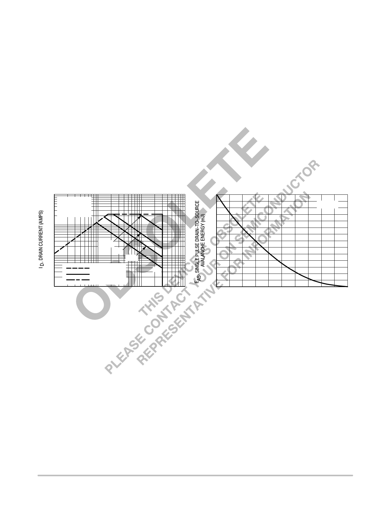
SAFE OPERATING AREA
The Forward Biased Safe Operating Area curves define
the maximum simultaneous drain−to−source voltage and
drain current that a transistor can handle safely when it is
forward biased. Curves are based upon maximum peak
junction temperature and a case temperature (TC) of 25°C.
Peak repetitive pulsed power limits are determined by using
the thermal response data in conjunction with the procedures
discussed in AN569, “Transient Thermal
Resistance−General Data and Its Use.”
Switching between the off−state and the on−state may
traverse any load line provided neither rated peak current
(IDM) nor rated voltage (VDSS) is exceeded, and that the
transition time (tr, tf) does not exceed 10 µs. In addition the
total power averaged over a complete switching cycle must
not exceed (TJ(MAX) − TC)/(RθJC).
A power MOSFET designated E−FET can be safely used
in switching circuits with unclamped inductive loads. For
reliable operation, the stored energy from circuit inductance
dissipated in the transistor while in avalanche must be less
than the rated limit and must be adjusted for operating
conditions differing from those specified. Although industry
practice is to rate in terms of energy, avalanche energy
capability is not a constant. The energy rating decreases
non−linearly with an increase of peak current in avalanche
and peak junction temperature.
Although many E−FETs can withstand the stress of
drain−to−source avalanche at currents up to rated pulsed
current (IDM), the energy rating is specified at rated
continuous current (ID), in accordance with industry
custom. The energy rating must be derated for temperature
as shown in the accompanying graph (Figure 13). Maximum
energy at currents below rated continuous ID can safely be
assumed to equal the values indicated.
1000
VGS = 20 V
SINGLE PULSE
TC = 25°C
100
100 µs
1 ms
10
10 ms
RDS(on) LIMIT
dc
THERMAL LIMIT
1
PACKAGE LIMIT
0.1
1
10
100
VDS, DRAIN−TO−SOURCE VOLTAGE (VOLTS)
Figure 11. Maximum Rated Forward Biased
Safe Operating Area
280
240
ID = 75 A
200
160
120
80
40
0
25
50
75
100
125
150
TJ, STARTING JUNCTION TEMPERATURE (°C)
Figure 12. Maximum Avalanche Energy versus
Starting Junction Temperature
http://onsemi.com
6
Share Link: 