BD7690FJ 查看數據表(PDF) - ROHM Semiconductor
零件编号
产品描述 (功能)
生产厂家
BD7690FJ Datasheet PDF : 26 Pages
| |||
BD7690FJ
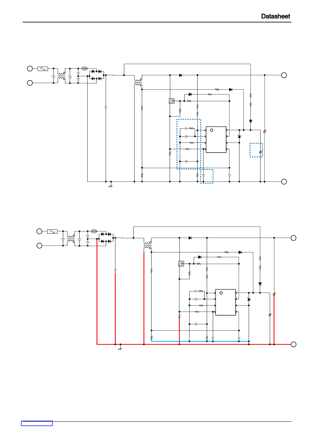
Attention in the board design
About parts placement
Please locate the parts in the Fig.23 inside dot line near the IC. In addition, please do parts placement to avoid the interference
with switching lines and high current lines such as inductor, DRAIN.
F1
L1
L
TH1
D1
C3
C1
C2
N
C4
C5
1uF
T1
250uH
RZCDH
100kΩ
D5
M1
RGS1
10kΩ
DOUT
ROUTE
100Ω
RVSH1
1.5MΩ
RVSH2
82kΩ
CEO2 REO
1uF 68kΩ
CEO1
0.47uF
RRT
150kΩ
ROCP1
0.18Ω
RCSF
1kΩ
RVCC
220Ω
ROUT
15Ω
DVCC
RSTR1
220kΩ
RSTR2
220kΩ
VOUT +
U1
VS
VCC
EO
OUT
BD7690FJ
RT
GND
CS
ZCD
DSTR
DZ1
CO
220uF
CVCC2
50uF
CVS
1000pF
RZCDL
20kΩ
RVSL
10kΩ
CCSF
100pF
CZCD
N/A
GND
GND
Figure 23. Parts placement
About GND wiring guidance
The red line of Fig.24 becomes the GND lines which large current flows. Each line independence wires it, and please wire it
briefly and thickly. A blue line is ICGND. Please make a common use ICGND and GND of IC outskirts parts.
F1
L1
L
TH1
D1
C3
C1
C2
N
C4
C5
1uF
T1
250uH
RZCDH
100kΩ
D5
M1
RGS1
10kΩ
DOUT
ROUTE
100Ω
RVSH1
1.5MΩ
RVSH2
82kΩ
CEO2 REO
1uF 68kΩ
CEO1
0.47uF
RRT
150kΩ
ROCP1
0.18Ω
RCSF
1kΩ
VOUT +
RVCC
220Ω
ROUT
15Ω
DVCC
RSTR1
220kΩ
RSTR2
220kΩ
U1
VS
VCC
EO
OUT
BD7690FJ
RT
GND
CS
ZCD
DSTR
DZ1
CO
220uF
CVCC2
50uF
RZCDL
20kΩ
CVS
1000pF
RVSL
10kΩ
CCSF
100pF
CZCD
N/A
GND
GND
Figure 24. GND line layout
www.rohm.com
© 2016 ROHM Co., Ltd. All rights reserved.
TSZ22111 • 15 • 001
16/22
TSZ02201-0F2F0A200280-1-2
27. Mar. 2017 Rev.002
Share Link: 