ISL95871C 查看數據表(PDF) - Renesas Electronics
零件编号
产品描述 (功能)
生产厂家
ISL95871C Datasheet PDF : 26 Pages
| |||
ISL95871C
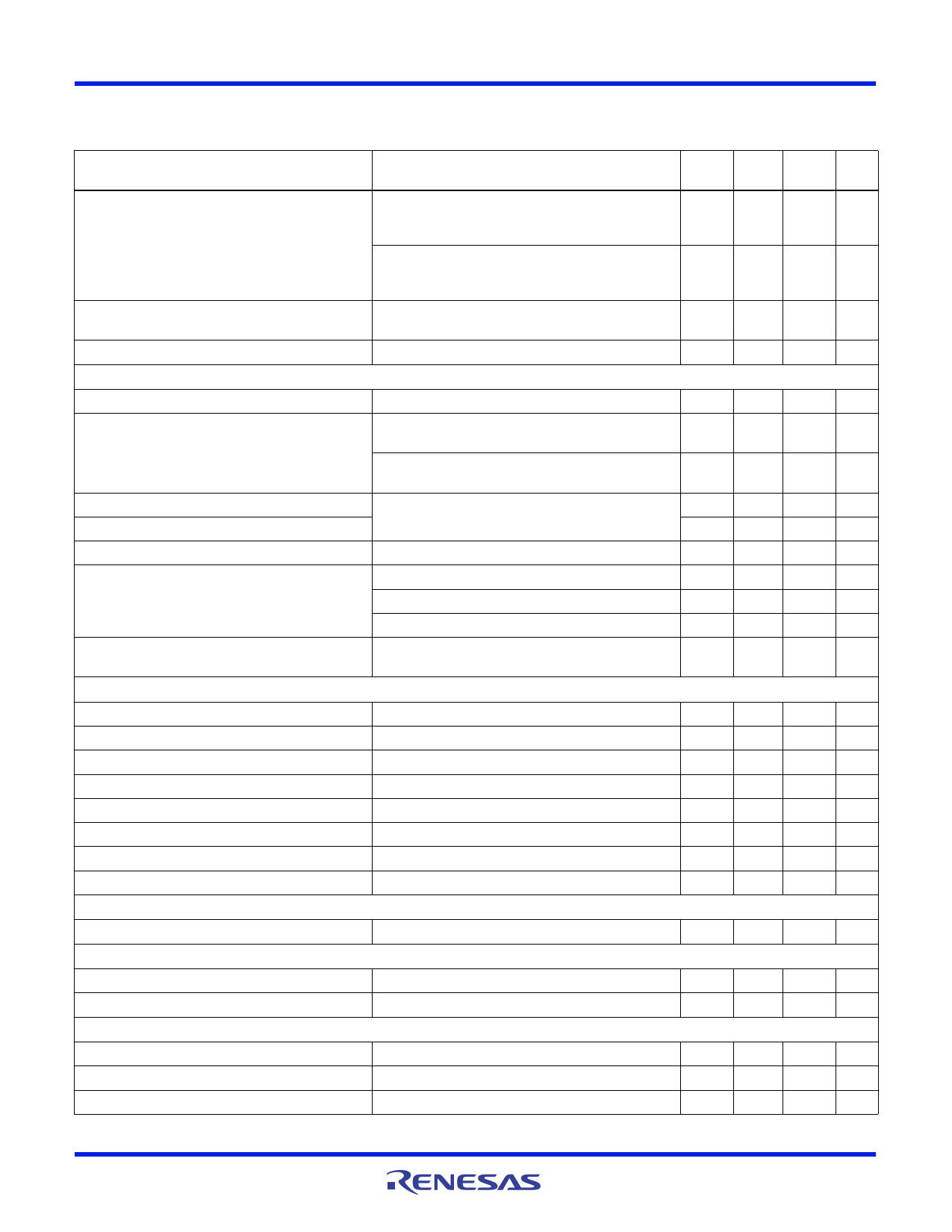
Electrical Specifications VIN = DCIN = VCSIP = VCSIN = 19V, VCSOP = VCSON = 12V, VDDP = 5.1V, VBOOT - VPHASE = 5V,
AGND = PGND = 0V, VDDSMB = 5V. All typical specifications TA = +25°C. Boldface limits apply over the junction temperature range, -10°C to
+125°C. (Continued)
PARAMETER
CONDITIONS
MIN
MAX
(Note 6) TYP (Note 6) UNITS
Battery Quiescent Current
Adapter Quiescent Current
VIN Leakage Current
Adapter present, not charging,
ICSOP + ICSON + IPHASE + IFB
VPHASE = VCSON = VCSOP = VDCIN = 19V, VACIN = 5V
Adapter Absent
ICSOP + ICSON + IPHASE + ICSIP + ICSIN + IFB
VPHASE = VCSON = VCSOP = 19V, VDCIN = 0V
IDCIN + ICSIP + ICSIN
Vadapter = 8V to 22V
PHASE = 0V, VIN = 22V
0.1
2
µA
0.1
2
µA
2.5
5
mA
0.3
1.5 µA
INPUT CURRENT REGULATION
CSIP to CSIN Full-Scale Current-Sense Voltage
Input Current Accuracy
VCSIP = 19V
RS1 = 10m (see Figure 4)
Adapter Current = 11008mA or 3584mA
106.7 110.08 113.3 mV
-3
3
%
RS1 = 10m (see Figure 4)
Adapter Current = 2048mA
-5
5
%
Input Current Limit Gain Error
Based on InputCurrent = 1024mA and 11008mA
-2
2
%
Input Current Limit Offset
-1
1
mV
ICM Gain
ICM Accuracy
ICM Load regulation
VCSIP-VCSIN = 110mV
VCSIP-VCSIN = 110mV
VCSIP-VCSIN = 55mV or 35mV
VCSIP-VCSIN = 20mV
VCSIP-VCSIN = 0.1V,
ICM load from zero to 500µA
19.9
V/V
-2.5
2.5
%
-4
4
%
-8
8
%
10 mV
SUPPLY AND LINEAR REGULATOR
VDDP Output Voltage
VDDP Load Regulation
VDDSMB UVLO Rising
8.0V < VDCIN < 22V, no load
0 < IVDDP < 30mA
4.95 5.1 5.23 V
35
100 mV
2.3
2.5 2.61
V
VDDSMB UVLO Falling
2.2
2.4
2.5
V
VDDSMB UVLO Hysteresis
100
mV
VDD UVLO Rising
4.25 4.5 4.65 V
VDD UVLO Hysteresis
150 280 400 mV
VDDSMB Quiescent Current
VDDP = SCL = SDA = 5.5V
20
27
µA
VOLTAGE REFERENCE
VREF Output Voltage
ACOK
0 < IVREF < 300µA
3.168 3.2 3.232 V
ACOK Sink Current
ACOK Leakage Current
ACIN
VACOK = 0.4V, ACIN = 1.5V
VACOK = 5.5V, ACIN = 2.5V
2
8
mA
1
µA
ACIN Rising Threshold
3.15 3.2 3.28 V
ACIN Threshold Hysteresis
40
60
90 mV
ACIN Input Leakage Current
ACIN = 3.7V
1
µA
FN6856 Rev 2.00
June 8, 2011
Page 7 of 26
Share Link: 