HIP6500CB 查看數據表(PDF) - Intersil
零件编号
产品描述 (功能)
生产厂家
HIP6500CB Datasheet PDF : 15 Pages
| |||
HIP6500
SOFT-START INTO ACTIVE STATES (S0, S1)
If both S3 and S5 are logic high at the time the 5VSB is
applied, the HIP6500 will assume active state wake-up and
keep off the controlled external transistors and the VCLK
output until some time (typically 25ms) after the ATX’s main
outputs used by the application (3.3V, 5V, and 12V) exceed
the set thresholds. This time-out feature is necessary in order
to insure the main ATX outputs are stabilized. The time-out
also assures smooth transitions from sleep into active when
sleep states are being supported. 3.3VSB output, whose
operation is only dependent on 5VSB presence, will come up
right as bias voltage reaches POR level.
During sleep to active state transitions from conditions
where the outputs are initially 0V (such as S5 to S0 transition
with EN3VDL = 1 and EN5VDL = 0, or simple power-up
sequence directly into active state), the 3VDUAL and
5VDUAL outputs go through a quasi soft-start by being pulled
high through the body diodes of the N-Channel MOSFETs
connected between these outputs and the 3.3V and 5V ATX
outputs. Figure 10 shows this start-up.
5VSB is already present when the main ATX outputs are
turned on at time T0. As a result of +3.3VIN and +5VIN
ramping up, the 3.3VDUAL and 5VDUAL output capacitors
charge up through the body diodes of Q3 and Q5,
respectively (see Figure 3). At time T1, all main ATX outputs
exceed the HIP6500’s undervoltage thresholds, and the
internal 25ms (typical) timer is initiated. At T2 the time-out
initiates a soft-start, and the memory and clock outputs are
ramped-up, reaching regulation limits at time T3.
Simultaneous with the beginning of the memory and clock
voltage ramp-up, at time T2, the DLA pin is pulled high,
turning on Q3 and Q5 in the process, and bringing the
3.3VDUAL and 5VDUAL outputs in regulation. Shortly after
time T3, as the SS voltage reaches 2.75V, the soft-start
capacitor is quickly discharged down to approximately
2.45V, where it remains until a valid sleep state request is
received from the system.
Fault Protection
All the outputs are monitored against undervoltage events. A
severe overcurrent caused by a failed load on any of the
outputs, would, in turn, cause that specific output to
suddenly drop. If any of the output voltages drop below 80%
(typical) of their set value, such event is reported by having
the FAULT/MSEL pin pulled to 5V. Additionally, exceeding
the maximum current rating of an integrated regulator
(output with pass regulator on chip) can lead to output
voltage drooping; if excessive, this droop can ultimately trip
the under-voltage detector and send a FAULT signal to the
computer system.
A FAULT condition occurring on an output when controlled
through an external pass transistor will only set off the
FAULT flag, and it will not shut off or latch off any part of the
circuit. A FAULT condition occurring on an output when
controlled through an internal pass transistor, will set off the
FAULT flag, and it will shut off the faulting regulator only. If
shutdown or latch off of the entire circuit is desired in case of
a fault, regardless of the cause, this can be achieved by
externally pulling or latching the SS pin low. Pulling the SS
pin low will also force the FAULT pin to go low and reset an
internally latched-off output.
Special consideration is given to the initial start-up sequence.
If, following a 5VSB POR event, the 3.3VSB output is ramped
up and is subject to an undervoltage event before the
remainder of the controlled voltages have been brought up,
then the FAULT output goes high and the entire IC latches off.
Latch-off condition can be reset by cycling the bias power
(5VSB). Undervoltage events on the 3.3VSB output at any
other times are handled according to the description found in
the second paragraph under the current heading.
Another condition that could set off the FAULT flag is chip
over-temperature. If the HIP6500 reaches an internal
temperature of 140oC (typical), the FAULT flag is set off, but
the chip continues to operate until the temperature reaches
155oC (typical), when unconditional shutdown of all outputs
takes place. Operation resumes at 140oC and the
temperature cycling occurs until the fault-causing condition
is removed.
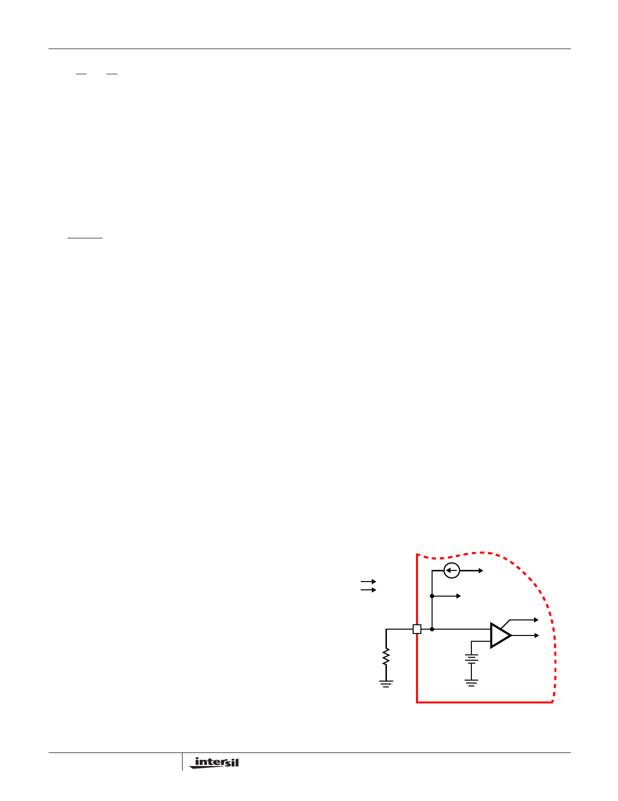
Output Voltages
The output voltages are internally set and do not require any
external components. Selection of the VMEM memory
voltage is done by means of an external resistor connected
between the FAULT/MSEL pin and ground. An internal 40µA
(typical) current source creates a voltage drop across this
resistor. Following every 3.3VSB ramp-up or chip reset (see
Soft-Start Circuit), this voltage is compared with an internal
reference and the setting is latched in. Based on this
comparison, the output voltage is set at either 2.5V (RSEL =
1kΩ), or 3.3V (RSEL = 10kΩ). It is very important that no
capacitor is connected to the FAULT/MSEL pin; the
presence of a capacitive element at this pin can lead to false
memory voltage selection. See Figure 11 for details.
RSEL
1kΩ
10kΩ
VMEM
2.5V
3.3V
FAULT/MSEL
RSEL
40µA
5VSB
MEM VOLTAGE
SELECT COMP
+
-
+
0.2V
-
FIGURE 11. 2.5/3.3VMEM OUTPUT VOLTAGE SELECTION
CIRCUITRY DETAILS
4-10
Share Link: 