ISL6131 查看數據表(PDF) - Renesas Electronics
零件编号
产品描述 (功能)
生产厂家
ISL6131 Datasheet PDF : 15 Pages
| |||
ISL6131, ISL6132
Ordering Information
PART
NUMBER
(Notes 2, 3)
PART
MARKING
TEMP.
RANGE
(°C)
PACKAGE
(Pb-free)
PKG.
DWG. #
ISL6131IRZA
(Note 1)
61 31IRZ -40 to +85 24 Ld 4x4 QFN L24.4x4
ISL6132IRZA
(Note 1)
61 32IRZ -40 to +85 24 Ld 4x4 QFN L24.4x4
ISL6131EVAL1Z Evaluation Board
ISL6132EVAL1Z Evaluation Board
NOTES:
1. Add “-T*” suffix for tape and reel. Please refer to TB347 for details on
reel specifications.
2. These Intersil Pb-free plastic packaged products employ special
Pb-free material sets, molding compounds/die attach materials, and
100% matte tin plate plus anneal (e3 termination finish, which is
RoHS compliant and compatible with both SnPb and Pb-free
soldering operations). Intersil Pb-free products are MSL classified at
Pb-free peak reflow temperatures that meet or exceed the Pb-free
requirements of IPC/JEDEC J STD-020.
3. For Moisture Sensitivity Level (MSL), please see device information
page for ISL6131, ISL6132. For more information on MSL, please see
Tech Brief TB363.
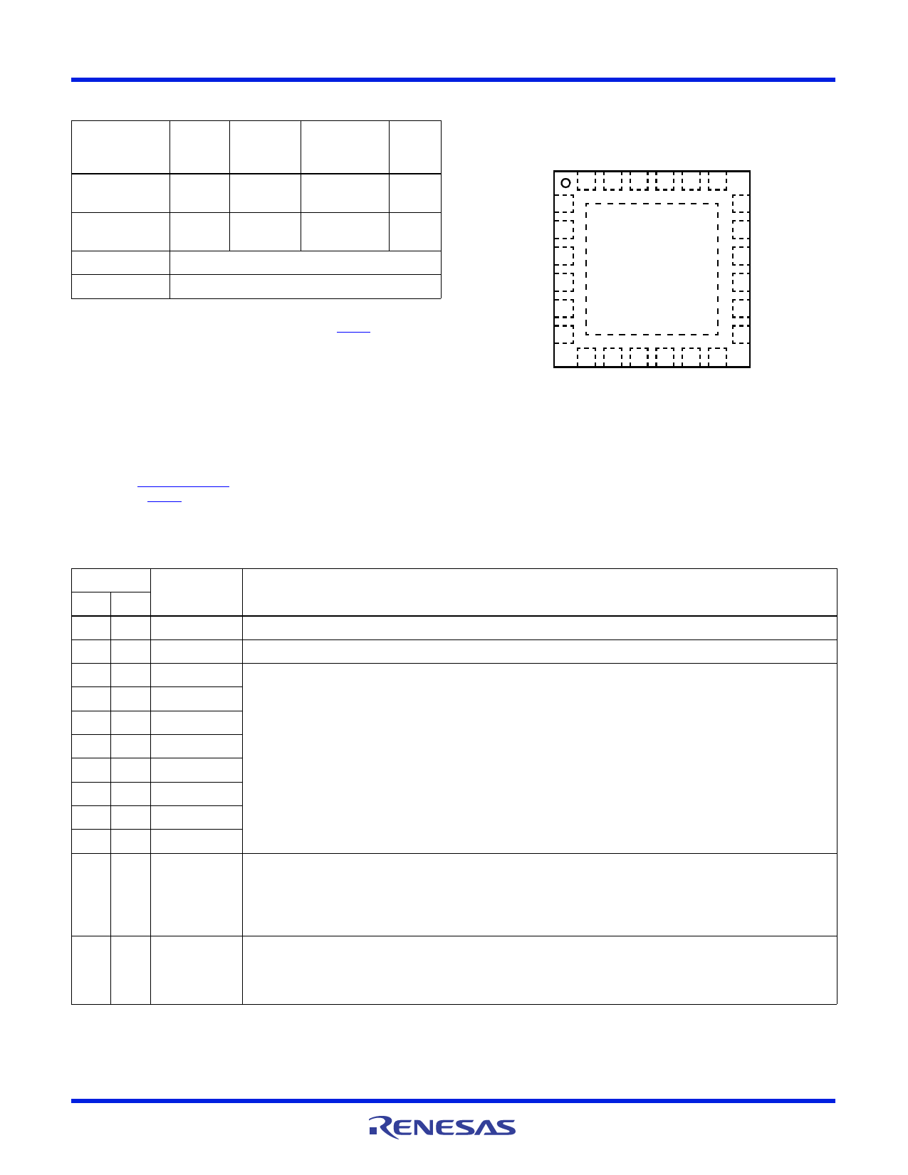
Pin Configuration
ISL6131, ISL6132
(24 LD QFN)
TOP VIEW
24 23 22 21 20 19
1
18
2
17
3
16
PD
4
15
5
14
6
13
7 8 9 10 11 12
Pin Descriptions
PIN
6131 6132
23 23
10 10
20 NA
12 NA
17 NA
14 NA
NA 12
NA 20
NA 17
NA 14
24 24
NA 9
PIN NAME
VDD
GND
VMON_A
VMON_B
VMON_C
VMON_D
OVMON_1
UVMON_1
UVMON_2
OVMON_2
PGOOD
PGOOD2
FUNCTION DESCRIPTION
Bias IC from nominal 1.5V to 5V
IC ground
On the ISL6131, these inputs provide a programmable UV threshold referenced to an internal 0.633V. The related
STATUS output asserts when the related input > internal reference voltage.
On the ISL6132, these inputs provide a programmable UV and OV threshold referenced to an internal 0.633V
reference. In the ‘AB’ pair, VMON_A is the UV input, and VMON_B is the OV input. In the ‘CD’ pair, VMON_C is the UV
input, and VMON_D is the OV input.
These inputs have a 30µs glitch filter to prevent PGOOD reset caused by a transient.
On the ISL6131, PGOOD is the Boolean AND function of all four STATUS outputs.
On the ISL6132, PGOOD is for the AB pair and signals high when the monitored voltage is within the specified window
and the A and B STATUS output states are correct.
This is an open-drain output and is to be pulled high to the appropriate level with an external resistor to a VDD
maximum level.
PGOOD2 is for the CD pair and signals high when the monitored voltage is within the specified window and when the
C and D STATUS output states are correct.
This is an open-drain output and is to be pulled high to the appropriate level with an external resistor to a VDD
maximum level.
FN9119 Rev 6.00
February 11, 2014
Page 2 of 15
Share Link: 