UPD78218ACW(A)-XXX 查看數據表(PDF) - NEC => Renesas Technology
零件编号
产品描述 (功能)
生产厂家
UPD78218ACW(A)-XXX Datasheet PDF : 66 Pages
| |||
µPD78217A, 78218A
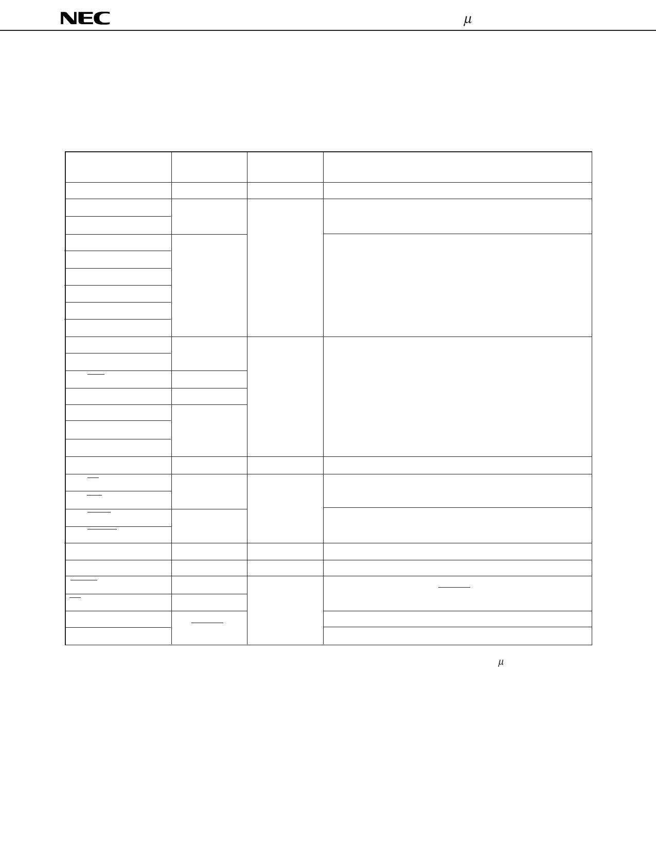
2.3 PIN I/O CIRCUITS AND UNUSED PIN CONNECTION
The input/output circuit type of each pin and recommended connection of unused pins are shown in Table 2-1.
For the input/output circuit configuration of each type, see Fig. 2-1.
Table 2-1 Input/Output Circuit Type of Each Pin
Pin Name
P00 to P07
P20/NMI
P21/INTP0
P22/INTP1
P23/INTP2/CI
P24/INTP3
P25/INTP4/ASCK
P26/INTP5
P27/SI
P30/RXD
P31/TXD
P32/SCK
P33/SB0/SO
P34/TO0 to P37/TO3
P40/AD0 to P47/AD7
P50/A8 to P57/A15
P60/A16 to P63/A19
P64/RD
P65/WR
P66/WAIT/AN6
P67/REFRQ/AN7
P70/AN0 to P75/AN5
ASTB
RESET
EA
AVREF
AVSS
Input/Output
Circuit Type
4
2
2-A
I/O
Output
Input
Unused Pin Connection
Leave open.
Connected to VDD or VSS .
Connected to VDD .
5-A
8-A
10-A
5-A
Input/output
Input
Output
: Connected to VDD.
: Leave open.
4
Output
Leave open.
5-A
Input/output Input
: Connected to VDD.
Output
: Leave open.
11
Input
: Connected to VDD.Note
Output
: Leave open.
9
Input
Connected to VSS .
4
Output
Leave open.
2
Input
1
Connected to VSS or VDD .Note
Connected to VSS .
Note A voltage outside the range AVSS to AVREF should not be applied, as this may damage the µPD78217A/78218A.
Caution
If the input/output mode is undefined for the input/output dual-function pins, connect these pins to
VDD via a resistor of several ten kΩ.
(Especially if the reset input pin exceeds the low-level input voltage at power-on or in case of input/
output switching by software.)
Remark The type numbers are standardized for 78K series, therefore they are not always consecutive numbers
for each product (some circuits are not incorporated).
13
Share Link: 