ICS8701CYIT 查看數據表(PDF) - Integrated Device Technology
零件编号
产品描述 (功能)
生产厂家
ICS8701CYIT Datasheet PDF : 14 Pages
| |||
ICS8701I
LOW SKEW, ÷1, ÷2
CLOCK GENERATOR
GENERAL DESCRIPTION
The ICS8701I is a low skew, ÷1, ÷2 Clock Generator. The
low impedance LVCMOS outputs are designed to drive 50Ω
series or parallel terminated transmission lines. The
effective fanout can be increased from 20 to 40 by utilizing
the ability of the outputs to drive two series terminated lines.
The divide select inputs, DIV_SELx, control the output
frequency of each bank. The outputs can be utilized in the ÷1,
÷2 or a combination of ÷1 and ÷2 modes. The bank enable
inputs, BANK_EN0:1, support enabling and disabling each
bank of outputs individually. The master reset input, nMR/OE,
resets the internal frequency dividers and also controls the
active and high impedance states of all outputs.
The ICS8701I is characterized at 3.3V and mixed 3.3V input
supply, and 2.5V output supply operating modes. Guaranteed
bank, output and part-to-part skew characteristics make the
ICS8701I ideal for those clock distribution applications de-
manding well defined performance and repeatability.
FEATURES
• Twenty LVCMOS outputs, 7Ω typical output impedance
• LVCMOS / LVTTL clock input
• Maximum input frequency: 250MHz
• Bank enable logic allows unused banks to be disabled
in reduced fanout applications
• Bank skew: 200ps
• Output skew: 250ps
• Multiple frequency skew: 300ps
• Part-to-part skew: 600ps
• 3.3V or mixed 3.3V input, 2.5V output operating supply
• -40°C to 85°C ambient operating temperature
• Other divide values available on request
• Available in both standard and lead-free RoHS compliant
packages
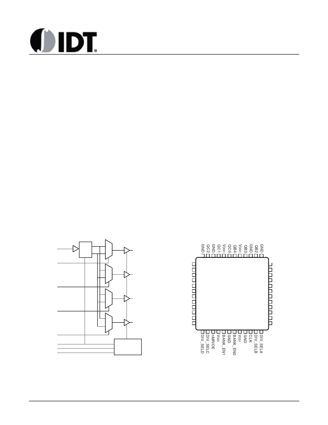
BLOCK DIAGRAM
÷1
CLK
÷2
DIV_SELA
DIV_SELB
DIV_SELC
DIV_SELD
nMR/OE
BANK_EN0
BANK_EN1
1
QA0:QA4
0
1
QB0:QB4
0
1
QC0:QC4
0
1
QD0:QD4
0
Bank Enable
Logic
PIN ASSIGNMENT
QC3
VDDO
QC4
QD0
VDDO
QD1
GND
QD2
GND
QD3
VDDO
QD4
48 47 46 45 44 43 42 41 40 39 38 37
1
36
2
35
3
34
4
33
5
32
6
ICS8701I
31
7
30
8
29
9
28
10
27
11
26
12
25
13 14 15 16 17 18 19 20 21 22 23 24
QB1
VDDO
QB0
QA4
VDDO
QA3
GND
QA2
GND
QA1
VDDO
QA0
48-Pin LQFP
7mm x 7mm x 1.4mm package body
Y Package
Top View
8701CYI
www.idt.com
1
REV. C JULY 27, 2010
Share Link: 