MMBTA13L 查看數據表(PDF) - ON Semiconductor
零件编号
产品描述 (功能)
生产厂家
MMBTA13L Datasheet PDF : 6 Pages
| |||
MMBTA13L, SMMBTA13L, MMBTA14L, SMMBTA14L
ELECTRICAL CHARACTERISTICS (TA = 25°C unless otherwise noted)
Characteristic
Symbol
Min
Max
Unit
OFF CHARACTERISTICS
Collector −Emitter Breakdown Voltage
(IC = 100 mAdc, VBE = 0)
Collector Cutoff Current
(VCB = 30 Vdc, IE = 0)
V(BR)CES
30
ICBO
−
Vdc
−
nAdc
100
Emitter Cutoff Current
(VEB = 10 Vdc, IC = 0)
ON CHARACTERISTICS (Note 3)
IEBO
nAdc
−
100
DC Current Gain
(IC = 10 mAdc, VCE = 5.0 Vdc)
MMBTA13, SMMBTA13
MMBTA14, SMMBTA14
(IC = 100 mAdc, VCE = 5.0 Vdc)
MMBTA13, SMMBTA13
MMBTA14, SMMBTA14
hFE
−
5000
−
10,000
−
10,000
−
20,000
−
Collector −Emitter Saturation Voltage
(IC = 100 mAdc, IB = 0.1 mAdc)
Base −Emitter On Voltage
(IC = 100 mAdc, VCE = 5.0 Vdc)
VCE(sat)
−
VBE
−
Vdc
1.5
Vdc
2.0
SMALL− SIGNAL CHARACTERISTICS
Current −Gain − Bandwidth Product (Note 4)
(IC = 10 mAdc, VCE = 5.0 Vdc, f = 100 MHz)
fT
MHz
125
−
Product parametric performance is indicated in the Electrical Characteristics for the listed test conditions, unless otherwise noted. Product
performance may not be indicated by the Electrical Characteristics if operated under different conditions.
3. Pulse Test: Pulse Width v 300 ms, Duty Cycle v 2.0%.
4. fT = |hfe| • ftest.
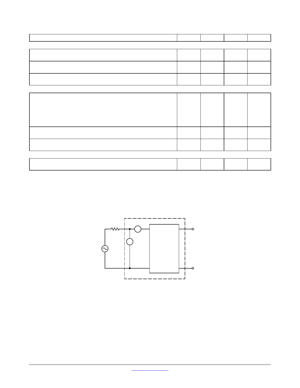
RS
in
en
IDEAL
TRANSISTOR
Figure 1. Transistor Noise Model
www.onsemi.com
2
Share Link: 