ICS8702BYT 查看數據表(PDF) - Integrated Circuit Systems
零件编号
产品描述 (功能)
生产厂家
ICS8702BYT Datasheet PDF : 12 Pages
| |||
Integrated
Circuit
Systems, Inc.
ICS8702
LOW SKEW ¸1, ¸2
CLOCK GENERATOR
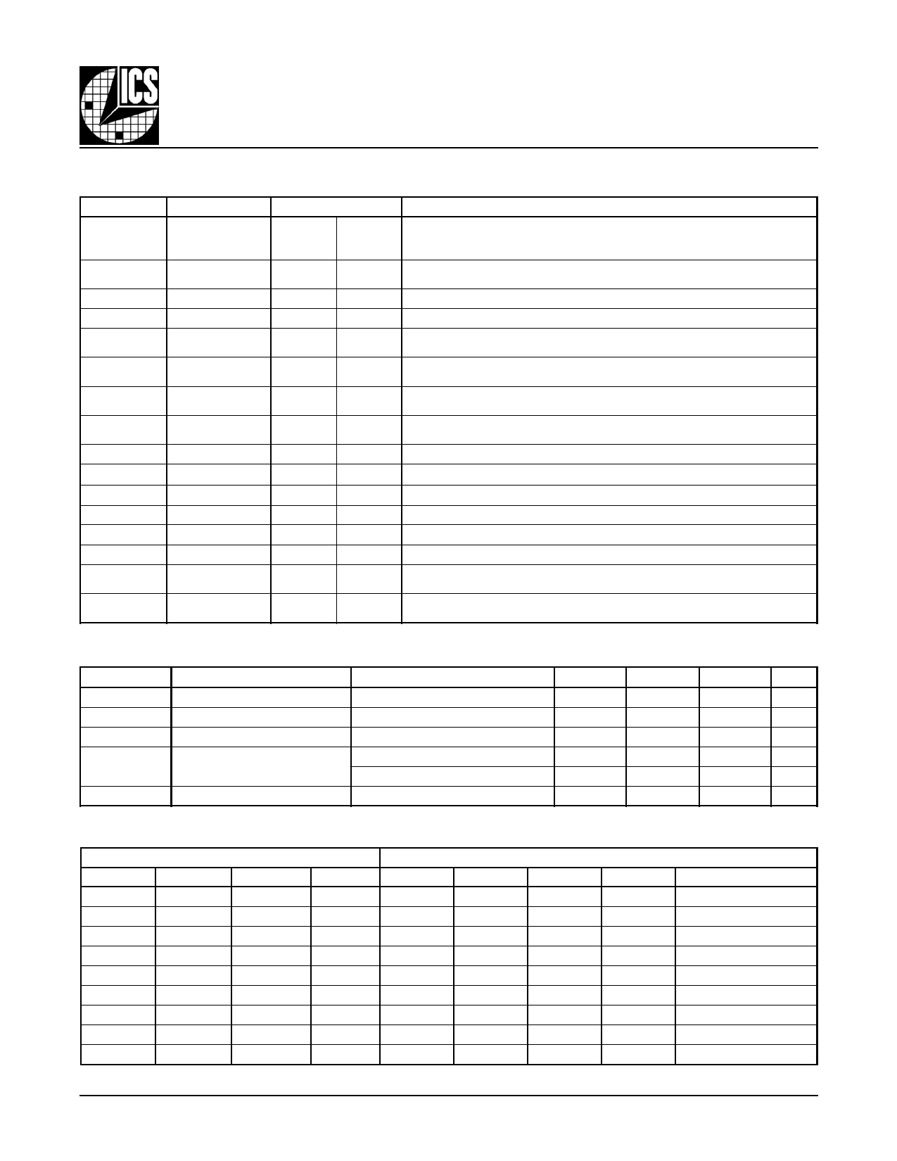
TABLE 1. PIN DESCRIPTIONS
Number
Name
2, 5, 11, 26,
32, 35, 41, 44
VDDO
7, 9, 28, 30,
37, 39, 46, 48
16, 20
18
25, 27, 29,
31, 33
34, 36, 38,
40, 42
43, 45, 47,
1, 3
4, 6, 8,
10, 12
22
21
13
14
23
24
17, 19
GND
VDDI
GND
QA0, QA1, QA2,
QA3, QA4
QB0, QB1, QB2,
QB3, QB4
QC0, QC1, QC2,
QC3, QC4
QD0, QD1, QD2,
QD3, QD4
CLK
nCLK
DIV_SELD
DIV_SELC
DIV_SELB
DIV_SELA
BANK_EN1,
BANK_EN0
15
nMR/OE
Type
Power
Description
Output power supply. Connect to 3.3V or 2.5V.
Power
Power
Power
Output
Output
Output
Output
Input
Input
Input
Input
Input
Input
Input
Input
Output power supply. Connect to ground.
Input power supply. Connect to 3.3V.
Input power supply. Connect to ground.
Bank A outputs. 7Ω typical output impedance.
Bank B outputs. 7Ω typical output impedance.
Bank C outputs. 7Ω typical output impedance.
Bank D outputs. 7Ω typical output impedance.
Pulldown Non-inverting differential clock input. Accepts any differential levels.
Pullup Inverting differential clock input. Accepts any differential levels.
Pullup Controls frequency division for bank D outputs. LVCMOS interface levels.
Pullup Controls frequency division for bank C outputs. LVCMOS interface levels.
Pullup Controls frequency division for bank B outputs. LVCMOS interface levels.
Pullup Controls frequency division for bank A outputs. LVCMOS interface levels.
Pullup
Pullup
Enables and disables outputs by banks. LVCMOS interface levels.
Asynchronous master reset. Resets clock dividers. Enables and disables all
outputs. LVCMOS interface levels.
TABLE 2. PIN CHARACTERISTICS
Symbol
CIN
RPULLUP
RPULLDOWN
Parameter
Input Capacitance
Input Pullup Resistor
Input Pulldown Resistor
CPD
Power Dissipation Capacitance
(per output)
ROUT
Output Impedance
Test Conditions
VDDI, VDDO = 3.465V
VDDI = 3.465V, VDDO = 2.625V
Minimum
Typical
51
51
7
Maximum
Units
pF
KΩ
KΩ
pF
pF
Ω
TABLE 3A. CONTROL INPUTS FUNCTION TABLE
Inputs
nMR/OE BANK_EN1 BANK_EN0 DIV_SELx
0
X
X
X
1
0
0
0
1
1
0
0
1
0
1
0
1
1
1
0
1
0
0
1
1
1
0
1
1
0
1
1
1
1
1
1
QA0 - QA4
Hi Z
Active
Active
Active
Active
Active
Active
Active
Active
QB0 - QB4
Hi Z
Hi Z
Active
Active
Active
Hi Z
Active
Active
Active
Outputs
QC0 - QC4 QD0 - QD4
Hi Z
Hi Z
Hi Z
Hi Z
Hi Z
Hi Z
Active
Hi Z
Active
Active
Hi Z
Hi Z
Hi Z
Hi Z
Active
Hi Z
Active
Active
Qx frequency
zero
fIN/2
fIN/2
fIN/2
fIN/2
fIN
fIN
fIN
fIN
8702
www.icst.com
2
REV. A - AUGUST 7, 2000
Share Link: 