AD5737 查看數據表(PDF) - Analog Devices
零件编号
产品描述 (功能)
生产厂家
AD5737 Datasheet PDF : 44 Pages
| |||
AD5737
PIN CONFIGURATION AND FUNCTION DESCRIPTIONS
PIN 1
INDICATOR
RSET_B 1
RSET_A 2
REFGND 3
REFGND 4
AD0 5
AD1 6
SYNC 7
SCLK 8
SDIN 9
SDO 10
DVDD 11
DGND 12
LDAC 13
CLEAR 14
ALERT 15
FAULT 16
AD5737
TOP VIEW
(Not to Scale)
48 COMPDCDC_C
47 IOUT_C
46 VBOOST_C
45 AVCC
44 SWC
43 GNDSWC
42 GNDSWD
41 SWD
40 AGND
39 SWA
38 GNDSWA
37
36
SGWNDBSWB
35 AGND
34 VBOOST_B
33 IOUT_B
Data Sheet
NOTES
1. NC = NO CONNECT. DO NOT CONNECT TO THIS PIN.
2. THE EXPOSED PADDLE SHOULD BE CONNECTED TO AGND, OR, ALTERNATIVELY,
IT CAN BE LEFT ELECTRICALLY UNCONNECTED. IT IS RECOMMENDED THAT
THE PADDLE BE THERMALLY CONNECTED TO A COPPER PLANE FOR ENHANCED
THERMAL PERFORMANCE.
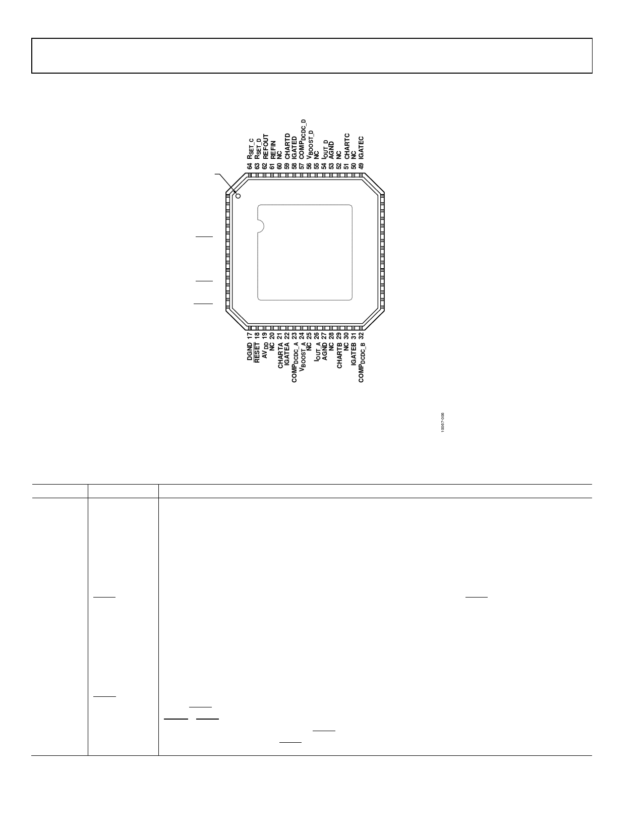
Figure 7. Pin Configuration
Table 6. Pin Function Descriptions
Pin No.
Mnemonic
Description
1
RSET_B
An external, precision, low drift, 15 kΩ current setting resistor can be connected to this pin to improve the
IOUT_B temperature drift performance. For more information, see the External Current Setting Resistor section.
2
RSET_A
An external, precision, low drift, 15 kΩ current setting resistor can be connected to this pin to improve the
IOUT_A temperature drift performance. For more information, see the External Current Setting Resistor section.
3
REFGND
Ground Reference Point for Internal Reference.
4
REFGND
Ground Reference Point for Internal Reference.
5
AD0
Address Decode for the Device Under Test (DUT) on the Board.
6
AD1
Address Decode for the DUT on the Board.
7
SYNC
Frame Synchronization Signal for the Serial Interface. Active low input. When SYNC is low, data is clocked
into the input shift register on the falling edge of SCLK.
8
SCLK
Serial Clock Input. Data is clocked into the input shift register on the falling edge of SCLK. The serial interface
operates at clock speeds of up to 30 MHz.
9
SDIN
Serial Data Input. Data must be valid on the falling edge of SCLK.
10
SDO
Serial Data Output. Used to clock data from the serial register in readback mode (see Figure 4 and Figure 5).
11
DVDD
Digital Supply Pin. The voltage range is from 2.7 V to 5.5 V.
12
DGND
Digital Ground.
13
LDAC
Load DAC. This active low input is used to update the DAC register and, consequently, the DAC outputs.
When LDAC is tied permanently low, the addressed DAC data register is updated on the rising edge of
SYNC. If LDAC is held high during the write cycle, the DAC input register is updated, but the DAC output
is updated only on the falling edge of LDAC (see Figure 3). Using this mode, all analog outputs can be
updated simultaneously. The LDAC pin must not be left unconnected.
Rev. B | Page 10 of 44
Share Link: 