900N20N 查看數據表(PDF) - Infineon Technologies
零件编号
产品描述 (功能)
生产厂家
900N20N Datasheet PDF : 9 Pages
| |||
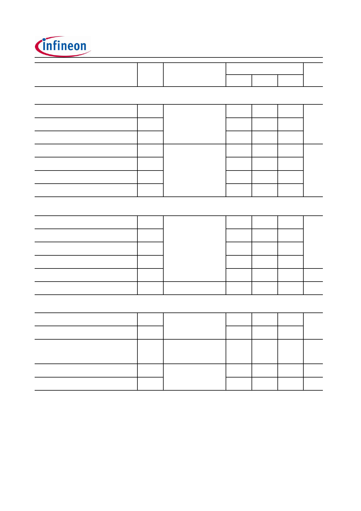
Parameter
Symbol Conditions
BSZ900N20NS3 G
min.
Values
typ.
Unit
max.
Dynamic characteristics
Input capacitance
Output capacitance
Reverse transfer capacitance
Turn-on delay time
Rise time
Turn-off delay time
Fall time
C iss
-
C oss
V GS=0 V, V DS=100 V,
f =1 MHz
-
C rss
-
t d(on)
-
tr
V DD=100 V,
-
V GS=10 V, I D=7.6 A,
t d(off)
R G=1.6 W
-
tf
-
690
920 pF
52
69
5.2
-
5
- ns
4
-
10
-
3
-
Gate Charge Characteristics4)
Gate to source charge
Gate to drain charge
Switching charge
Gate charge total
Gate plateau voltage
Output charge
Q gs
-
Q gd
-
Q sw
V DD=100 V, I D=7.6 A,
V GS=0 to 10 V
-
Qg
-
V plateau
-
Q oss
V DD=100 V, V GS=0 V
-
3.1
- nC
1.3
-
2.3
-
8.7
11.6
4.5
-V
20
26 nC
Reverse Diode
Diode continous forward current
Diode pulse current
IS
I S,pulse
T C=25 °C
-
-
15.2 A
-
-
61
Diode forward voltage
V SD
V GS=0 V, I F=15.2 A,
T j=25 °C
-
1
1.2 V
Reverse recovery time
Reverse recovery charge
t rr
V R=100 V, I F=I S,
Q rr
di F/dt =100 A/µs
-
86
- ns
-
309
- nC
4) See figure 16 for gate charge parameter definition
Rev. 2.2
page 3
2011-07-14
Share Link: 