XRT83VSH314 查看數據表(PDF) - Exar Corporation
零件编号
产品描述 (功能)
生产厂家
XRT83VSH314 Datasheet PDF : 80 Pages
| |||
REV. 1.0.1
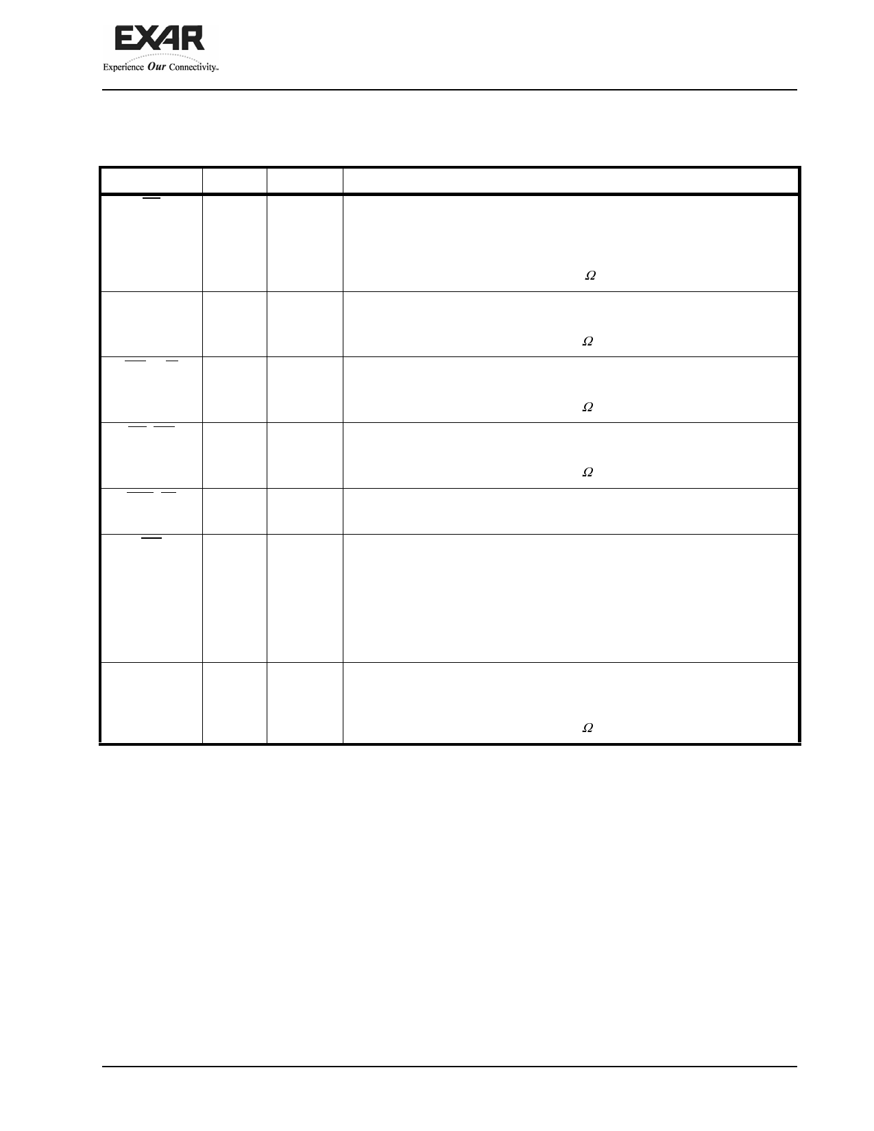
1.0 PIN DESCRIPTIONS
XRT83VSH314
14-CHANNEL T1/E1/J1 SHORT-HAUL LINE INTERFACE UNIT
MICROPROCESSOR
NAME
PIN
CS
A22
ALE_TS
C19
WR_R/W
A20
RD_WE
D18
RDY_TA
AA3
INT
B3
µPCLK
AB2
TYPE
I
I
I
I
O
O
I
DESCRIPTION
Chip Select Input
Active low signal. This signal enables the microprocessor interface by pulling
chip select "Low". The microprocessor interface is disabled when the chip
select signal returns "High".
NOTE: Internally pulled "High" with a 50k Ω resistor.
Address Latch Enable Input (Transfer Start)
See the Microprocessor section of this datasheet for a description.
NOTE: Internally pulled "Low" with a 50k Ω resistor.
Write Strobe Input (Read/Write)
See the Microprocessor section of this datasheet for a description.
NOTE: Internally pulled "Low" with a 50k Ω resistor.
Read Strobe Input (Write Enable)
See the Microprocessor section of this datasheet for a description.
NOTE: Internally pulled "Low" with a 50k Ω resistor.
Ready Output (Transfer Acknowledge)
See the Microprocessor section of this datasheet for a description.
Interrupt Output
Active low signal. This signal is asserted "Low" when a change in alarm status
occurs. Once the status registers have been read, the interrupt pin will return
"High". GIE (Global Interrupt Enable) must be set "High" in the appropriate
global register to enable interrupt generation.
NOTE: This pin is an open-drain output that requires an external 10KΩ pull-up
resistor.
Micro Processor Clock Input
In a synchronous microprocessor interface, µPCLK is used as the internal tim-
ing reference for programming the LIU.
NOTE: Internally pulled "Low" with a 50k Ω resistor.
4
Share Link: 