HT9011 查看數據表(PDF) - Holtek Semiconductor
零件编号
产品描述 (功能)
生产厂家
HT9011 Datasheet PDF : 7 Pages
| |||
Preliminary
HT9011
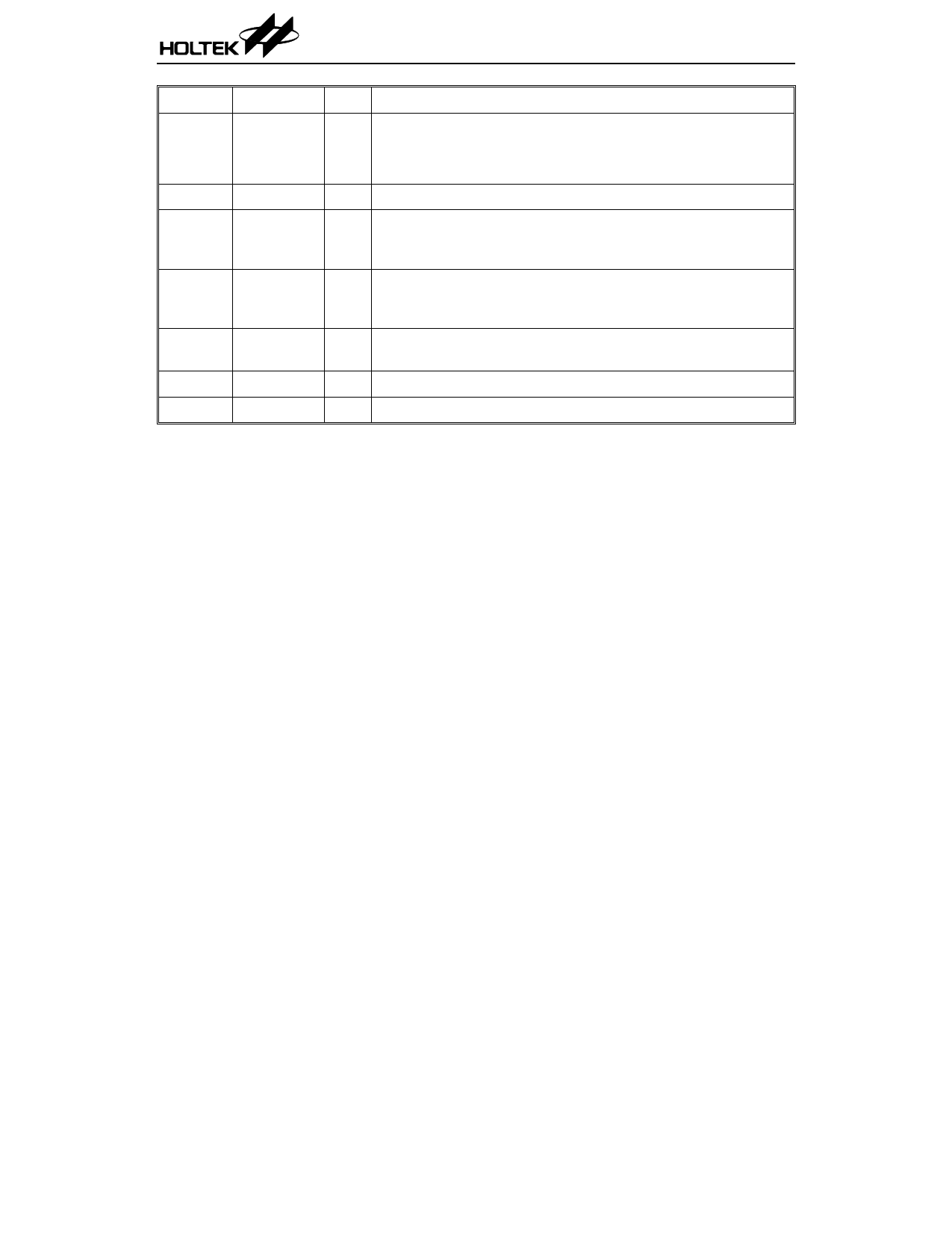
Pin No. Pin Name
14 CHG
15 FSKO
16 ALM
17 REGC
18 REGO
19 GND
20 MIXI
I/O
Description
Control pin for quick charge-discharge circuit.
I ²H² turn on quick charge-discharge
²L² turn off quick charge-discharge
O FSK NRZ data output
Output pin for Low Voltage Alarm
O At VCC@1.1V, this pin becomes ²H² (@VCC) and can indicate dete-
rioration of battery.
Control pin of external transistor for regulator of external power
O supply.
Externally connect the PNP transistor
O
Output voltage monitoring pin of regulator for external power
supply.
¾ Negative power supply, ground
I MIXER Input terminal
Absolute Maximum Ratings
Power Supply Voltage............VCC-0.3V to 4.0V
Operating Temperature range ........0°C to 45°C
Power Dissipation ..................................730mW
Storage Temperature.................-55°C to 150°C
Note: These are stress ratings only. Stresses exceeding the range specified under ²Absolute Maxi-
mum Ratings² may cause substantial damage to the device. Functional operation of this device
at other conditions beyond those listed in the specification is not implied and prolonged expo-
sure to extreme conditions may affect device reliability.
3
March 1, 2000
Share Link: 