CY8C4145AXI-432 查看數據表(PDF) - Cypress Semiconductor
零件编号
产品描述 (功能)
生产厂家
CY8C4145AXI-432 Datasheet PDF : 43 Pages
| |||
PSoC® 4: PSoC 4100 Family
Datasheet
35-Ball CSP
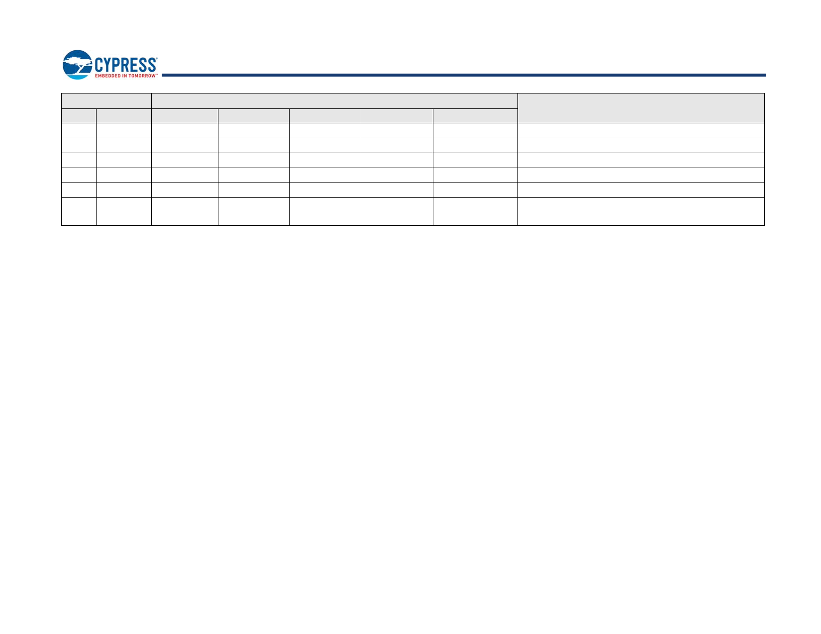
Pin
Name
Analog
C6
P1.2
ctb.oa0.out
D7
P1.3
ctb.oa1.out
D4
P1.4
ctb.oa1.inm
D5
P1.5
ctb.oa1.inp
D6
P1.6 ctb.oa0.inp_alt
E7 P1.7/VREF ctb.oa1.inp_alt
ext_vref
Alternate Functions for Pins
Alt 1
Alt 2
Alt 3
tcpwm3_p[1]
–
–
tcpwm3_n[1]
–
–
–
–
–
–
–
–
–
–
–
–
–
–
Alt 4
–
–
–
–
–
–
Pin Description
Port 1 Pin 2: gpio, lcd, csd, ctb, pwm
Port 1 Pin 3: gpio, lcd, csd, ctb, pwm
Port 1 Pin 4: gpio, lcd, csd, ctb
Port 1 Pin 5: gpio, lcd, csd, ctb
Port 1 Pin 6: gpio, lcd, csd
Port 1 Pin 7: gpio, lcd, csd, ext_ref
Descriptions of the Pin functions are as follows:
VDDD: Power supply for both analog and digital sections (where there is no VDDA pin).
VDDA: Analog VDD pin where package pins allow; shorted to VDDD otherwise.
VSSA: Analog ground pin where package pins allow; shorted to VSS otherwise
VSS: Ground pin.
VCCD: Regulated Digital supply (1.8 V ±5%).
Port Pins can all be used as LCD Commons, LCD Segment drivers, or CSD sense and shield pins can be connected to AMUXBUS A or B or can all be used as GPIO pins
that can be driven by firmware or DSI signals.
The following packages are supported: 48-pin TQFP, 44-pin TQFP, 40-pin QFN, and 28-pin SSOP.
Document Number: 001-87220 Rev. *J
Page 12 of 43
Share Link: 