LT1366(Rev_A) 查看數據表(PDF) - Linear Technology
零件编号
产品描述 (功能)
生产厂家
LT1366 Datasheet PDF : 20 Pages
| |||
LT1366/LT1367
LT1368/LT1369
TYPICAL APPLICATIONS
the 2 op amp loop to create a negative summing junction
at A1’s positive input1. The circuit has low sensitivities for
center frequency and Q, which are set with the following
equations:
ω02 = 1/(R1 • C1 • R2 • C2)
where,
R1 = 1/(ω0 • Q • C1) and R2 = Q/(ω0 • C2).
The DC bias applied to A2 and A4, half supply, is not
needed when split supplies are available. The circuit
swings rail-to-rail in the passband making it an excellent
anti-aliasing filter for ADCs. The amplitude response is flat
to 1kHz then rolls off at 80dB/decade.
1James Hahn, “State Variable Filter Trims Predecessor’s Component Count,” Electronics, April
21, 1982.
0
–20
– 40
– 60
– 80
100
GAIN
180
144
PHASE
108
72
36
0
–36
–72
–108
1k
FREQUENCY (Hz)
–144
–180
10k
1366 F09
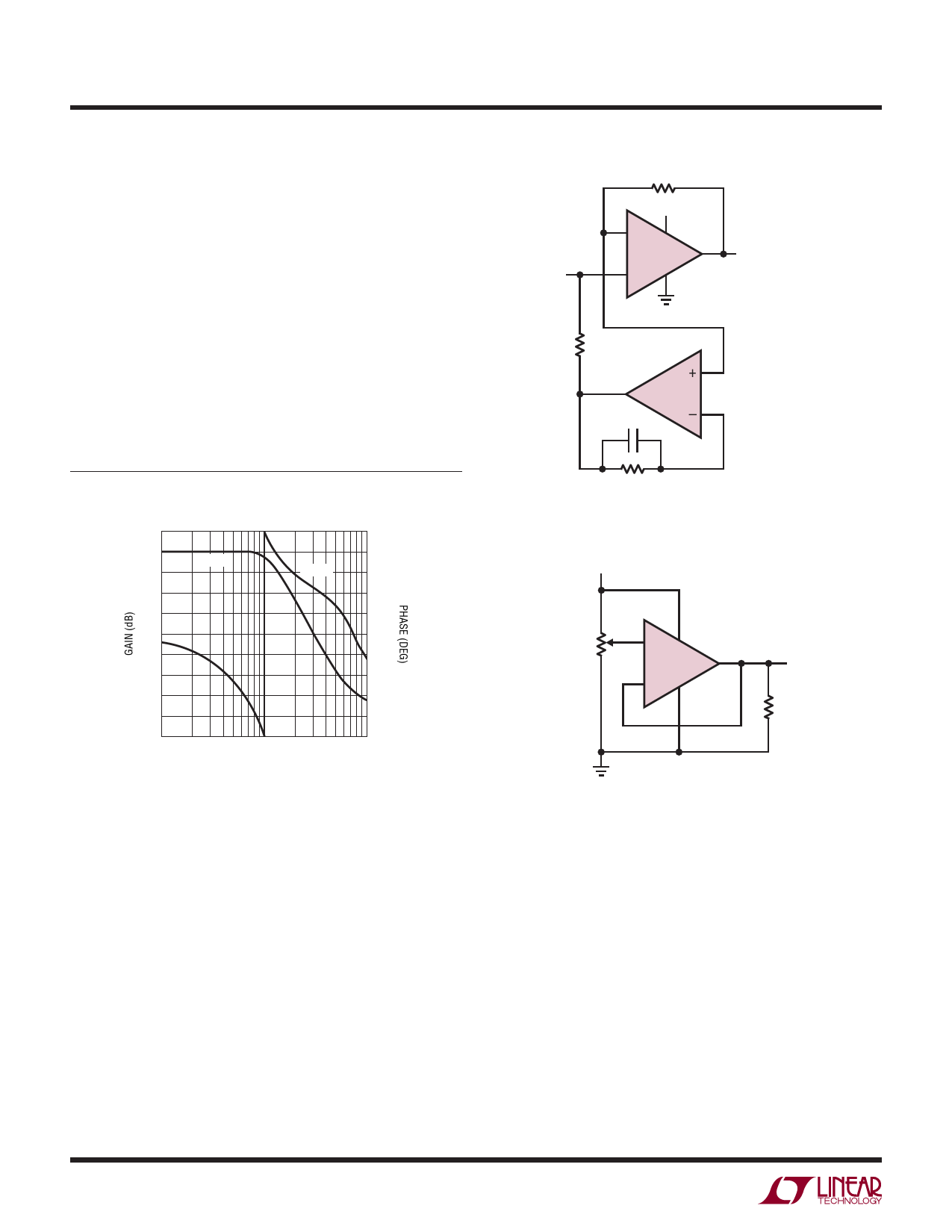
Figure 9. Frequency Response of 4th Order Butterworth Filter
10k
V+
2–
1
1/2 LT1366
VOUT
VIN
3+
SIGNAL AMP
1M
5
7
1/2 LT1366
22pF
CANCELLATION AMP
6
1M
1366 F10
Figure 10. Input Bias Current Cancellation
VCC
RP
+
10k
1/2 LT1366
–
RL
1366 F11
Figure 11. Rail-to-Rail Potentiometer Buffer
16
Share Link: 