WM9712CLGEFL/V 查看數據表(PDF) - Wolfson Microelectronics plc
零件编号
产品描述 (功能)
生产厂家
WM9712CLGEFL/V Datasheet PDF : 78 Pages
| |||
Production Data
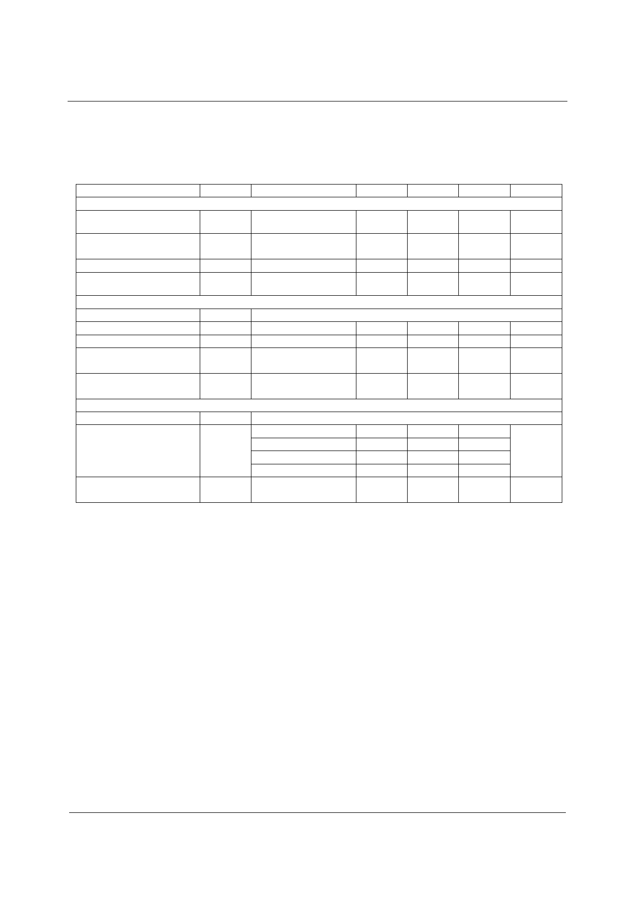
ELECTRICAL CHARACTERISTICS
WM9712L
AUDIO OUTPUTS
Test Conditions
DBVDD=3.3V, DCVDD = 3.3V, AVDD=HPVDD=SPKVDD =3.3V, TA = +25oC, 1kHz signal, fs = 48kHz, 18-bit audio data unless
otherwise stated.
PARAMETER
SYMBOL TEST CONDITIONS
MIN
TYP
MAX
UNIT
DAC to Line-Out (HPOUTL/R or MONOOUT with 10k / 50pF load)
Full-scale output
AVDD = 3.3V, PGA gains
1
set to 0dB
V rms
Signal to Noise Ratio
(A-weighted)
SNR
85
94
dB
Total Harmonic Distortion
THD
-3dB output
-87
-80
dB
Power Supply Rejection
PSRR
100mV, 20Hz to 20kHz
50
dB
signal on AVDD
Speaker Output (LOUT2/ROUT2 with 8 bridge tied load, INV=1)
Output Power
PO
Output power is very closely correlated with THD; see below.
Output Power at 1% THD
PO
400
mW
Abs. Max Output Power
POmax
500
mW
Total Harmonic Distortion
THD
PO=200mW
-66
dB
0.05
%
Signal to Noise Ratio
(A-weighted)
SNR
90
100
dB
Headphone Output (HPOUTL/R, OUT3 or LOUT2/ROUT2 with 16 or 32 load)
Output Power per channel
PO
Output power is very closely correlated with THD; see below.
Total Harmonic Distortion
THD
PO=10mW, RL=16
-76
dB
PO=10mW, RL=32
-73
PO=20mW, RL=16
-75
-70
PO=20mW, RL=32
-78
Signal to Noise Ratio
SNR
90
95
dB
(A-weighted)
Note:
1. All THD values are valid for the output power level quoted above – for example, at HPVDD=3.3V and RL=16, THD is
–76dB when output power is 10mW. Higher output power is possible, but will result in a deterioration in THD.
w
PD, Rev 4.6, November 2011
7
Share Link: 