SCAN182374A 查看數據表(PDF) - Fairchild Semiconductor
零件编号
产品描述 (功能)
生产厂家
SCAN182374A Datasheet PDF : 12 Pages
| |||
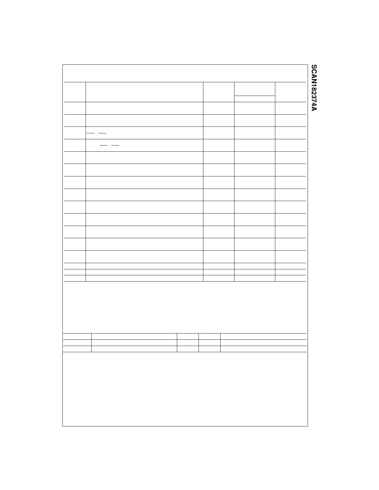
AC Operating Requirements
Scan Test Operation
VCC
TA = −40°C to +85°C
Symbol
Parameter
(V)
CL = 50 pF
Units
(Note 8)
Guaranteed Minimum
tS
Setup Time
Data to TCK (Note 9)
5.0
2.7
ns
tH
Hold Time
Data to TCK (Note 9)
5.0
3.1
ns
tS
Setup Time, H or L
AOE1, BOE1 to TCK (Note 10)
tH
Hold Time, H or L
TCK to AOE1, BOE1 (Note 10)
tS
Setup Time, H or L
Internal AOE, BOE to TCK (Note 11)
5.0
5.0
ns
5.0
1.8
ns
5.0
3.6
ns
tH
Hold Time, H or L
TCK to Internal AOE, BOE (Note 11)
5.0
2.1
ns
tS
Setup Time
ACP, BCP (Note 12) to TCK
5.0
3.4
ns
tH
Hold Time
TCK to ACP, BCP (Note 12)
5.0
1.8
ns
tS
Setup Time, H or L
TMS to TCK
5.0
8.7
ns
tH
Hold Time, H or L
TCK to TMS
5.0
1.8
ns
tS
Setup Time, H or L
TDI to TCK
5.0
6.4
ns
tH
Hold Time, H or L
TCK to TDI
5.0
3.2
ns
tW
Pulse Width TCK
H
8.2
5.0
ns
L
11.2
fMAX
Maximum TCK Clock Frequency
tPU
Wait Time, Power Up to TCK
tDN
Power Down Delay
Note 8: Voltage Range 5.0V ± 0.5V
5.0
50
MHz
5.0
100
ns
0.0
100
ms
Note 9: This delay represents the timing relationship between the data input and TCK at the associated scan cells numbered 0–8, 9–17, 18–26 and 27–35.
Note 10: Timing pertains to BSR 38 and 41 only.
Note 11: This delay represents the timing relationship between AOE/BOE and TCK for scan cells 36 and 39 only.
Note 12: Timing pertains to BSR 37 and 40 only.
Note: All Input Timing Delays involving TCK are measured from the rising edge of TCK.
Capacitance
TA = 25°C
Symbol
Parameter
Typ
CIN
Input Capacitance
5.8
COUT (Note 13) Output Capacitance
13.8
Note 13: COUT is measured at frequency f = 1 MHz, per MIL-STD-883B, Method 3012.
Units
pF
pF
VCC = 0.0V
VCC = 5.0V
Conditions
11
www.fairchildsemi.com
Share Link: 