TEA6811V 查看數據表(PDF) - Philips Electronics
零件编号
产品描述 (功能)
生产厂家
TEA6811V Datasheet PDF : 22 Pages
| |||
www.ti.com
TPS72501
TPS72515, TPS72516
TPS72518, TPS72525
SLVS341D – MAY 2002 – REVISED MARCH 2004
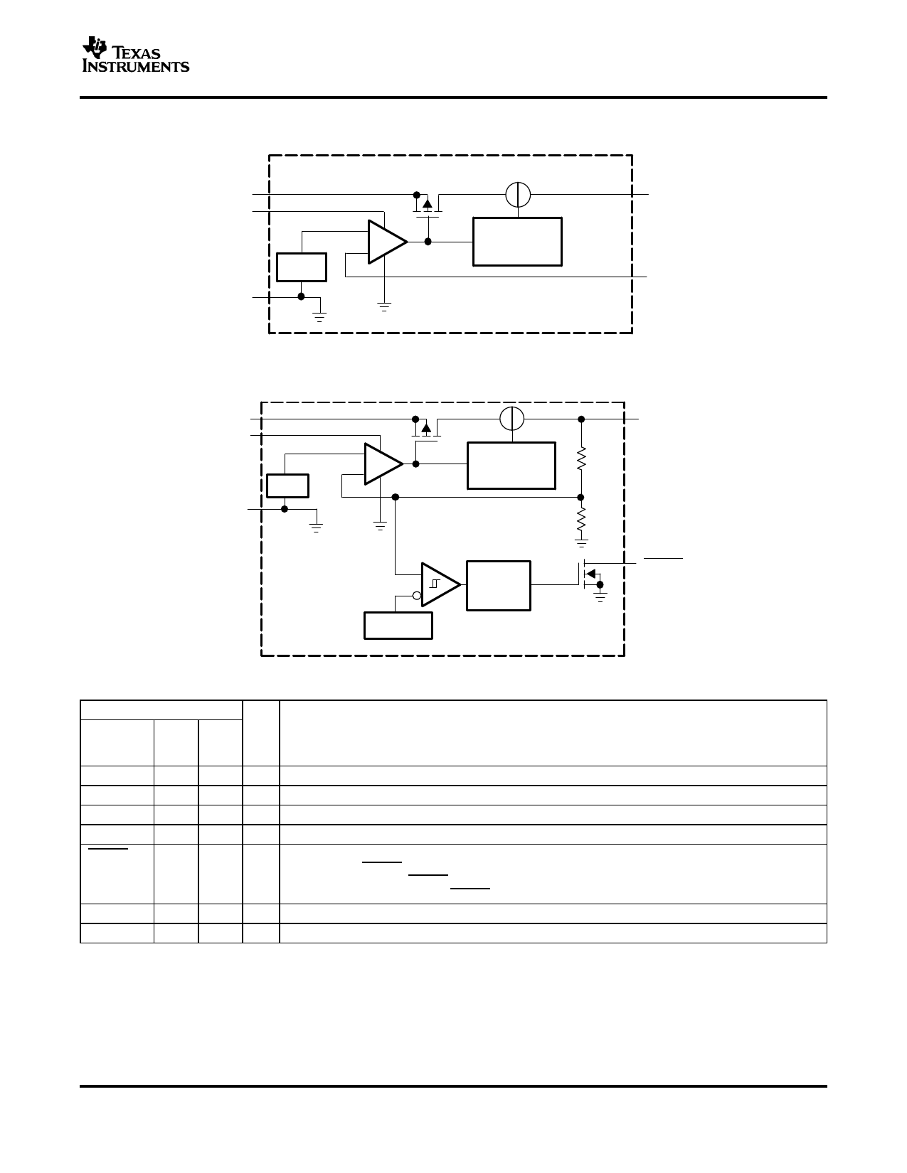
FUNCTIONAL BLOCK DIAGRAM—ADJUSTABLE VERSION
TPS72501
IN
EN
GND
1.220
Vref
Current
Limit/Thermal
Protection
OUT
FB
IN
EN
GND
FUNCTIONAL BLOCK DIAGRAM—FIXED VERSION
TPS72515/16/18/25
1.220
Vref
Current
Limit/Thermal
Protection
OUT
0.93 × Vref
Deglitch
and
Delay
RESET
TERMINAL
NAME
NO.
D
NO.D
CQ &
KTT
ENABLE
5
1
FB
2
GND 3, 6, 7 3
IN
8
2
RESET/FB —
5
NC
OUT
4
—
1
4
TERMINAL FUNCTIONS
I/O DESCRIPTION
I Enable input
Feedback
Ground
I Input supply voltage
O/I This terminal is the feedback point for the adjustable option TPS72501. For all other options, this
terminal is the RESET output terminal. When used with a pullup resistor, this open-drain output
provides the active low RESET signal when the regulator output voltage drops more than 5% below
its nominal output voltage. The RESET delay time is typically 50 ms.
No connection
O Regulated output voltage
5
Share Link: 