TDE1747FPT 查看數據表(PDF) - STMicroelectronics
零件编号
产品描述 (功能)
生产厂家
TDE1747FPT Datasheet PDF : 17 Pages
| |||
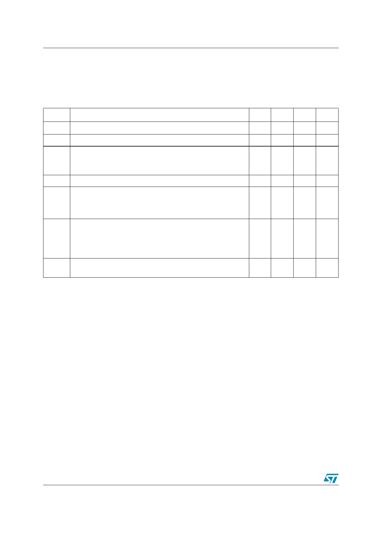
Electrical characteristics
2 Electrical characteristics
TDE1747
TJ = −25 to +85°C, VCC = 8 to 45 V, unless otherwise specified (note 1)
Table 3. Electrical characteristics
Symbol
Parameter
Min Typ Max Unit
VIO Input offset voltage(1)(2)
–
2
50 mV
IIB Input bias current
–
0.1 1.5 mA
Supply Current (VCC = +24V, IO = 0)
ICC High level
Low level
–
4
6
mA
–
2
4
mA
VI(max) Common–mode input voltage range
2
– VCC–2 V
Short–circuit Current Limit (TA = 25°C, VCC = +24V)
ISC RSC= 1.5Ω
RSC= ∞
–
480
–
mA
–
35
50 mA
VCC–VO
Output saturation voltage (output low)
(VI+– VI- ≥ 50mV, RSC = 0, IO = 300mA, )
TJ = + 25°C
TA = + 25°C
– 1.15 1.4
V
– 1.05 1.3
V
IOL
Output leakage current (output high)
(VO = 0, VCC = +24V, TA = + 25°C)
–
0.01 10
µA
1. For operating at high temperature, the TDE1747, must be derated based on a +150°C maximum junction temperature and
junction-ambient thermal resistance of 120°C/W for DIP-8 and 100°C/W for the SO14.
2. The offset voltage given is the maximum value of input voltage required to drive the output voltage within 2V of the ground
or the supply voltage.
4/17
Share Link: 