TDA1599 查看數據表(PDF) - Philips Electronics
零件编号
产品描述 (功能)
生产厂家
TDA1599 Datasheet PDF : 22 Pages
| |||
Philips Semiconductors
IF amplifier/demodulator for FM radio
receivers
Product specification
TDA1599
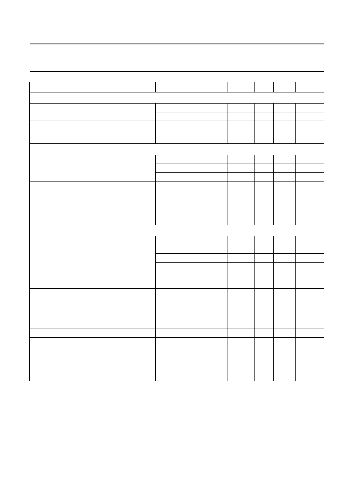
SYMBOL
PARAMETER
CONDITIONS
External muting
V16
muting voltage at I2 = 0
V20 ≤ 5 µV RMS; Fig.12
V20 = 1 mV RMS
S
steepness of control voltage
(slope: 100 µV ≤ V20 ≤ 100 mV)
20 ∆log V20 = 20 dB (∆V16 / ∆log V20)
Internal mute α = 20 log (∆V4(FM-MUTE-OFF)/ ∆V4(FM-MUTE-ON))
α
mute voltage
I16
current for capacitor (pin 16)
charge current
discharge current
charge current
discharge current
V16 ≥ VREF
V16 = 0.77VREF
V16 = 0.55VREF
V13 = 0 V
V13 = 0 V
V13 = VREF
V13 = VREF
Level detector
R6
output resistance
V6
output voltage at I2 = 0
output voltage at V2 = V5
∆V6
output voltage at detuning
TC
temperature coefficient
V20 ≤ 5 µV RMS; Fig.14
V20 = 1 mV RMS
±200 kHz detuning
V20 ≤ 5 µV RMS
±45 kHz detuning
∆f
S
∆V6/∆f
S
detuning frequency
steepness of control voltage
(slope: 50 µV ≤ V20 ≤ 50 mV)
20 ∆log V20 = 20 dB (∆V6 / ∆log V20)
slope of output voltage at detuning
level shift adjustments
V6 = 1.8 V; Fig.13
∆f = 125 ± 20 kHz
range by pin 2
gain
range by pin 2
gain
±∆V6/VREF
−∆V6/∆V2
±∆V16/VREF
−∆V16/∆V2
MIN. TYP. MAX. UNIT
1.45
1.75 2.05 V
3.0
3.45 3.9 V
−
0.85 −
V/dec
−
0
−
dB
1.5
−
4.5 dB
−
20 −
dB
−
−8 −
µA
−
+120 −
µA
−
−100 −
µA
−
+120 −
µA
−
−
500 Ω
0.1
−
1.1 V
3.0
−
4.2 V
1.2
1.5 1.8 V
−
−
0.3 V
−
−
0.2 V
−
3.3 −
mV/VK
90
−
160 kHz
1.4
1.7 2.0 V/dec
−
35 −
0.42
0.5 −
−
1.7 −
0.21
0.25 −
−
0.85 −
mV/kHz
V/V
V/V
V/V
V/V
May 1994
8
Share Link: 