STV9382 查看數據表(PDF) - STMicroelectronics
零件编号
产品描述 (功能)
生产厂家
STV9382
STMicroelectronics
STV9382 Datasheet PDF : 10 Pages
| |||
Absolute Maximum Ratings
OPTIMWATTTM STV9382
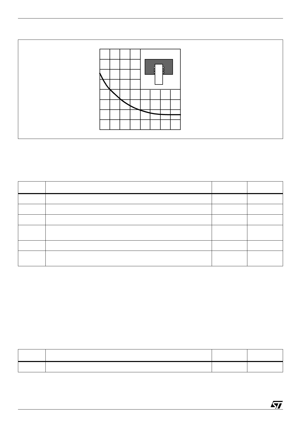
Figure 2: Thermal Resistance with “On-board” Square Heatsink vs. Copper Area
RthJA
(°C/W)
70
Copper Area 35 µm
Thickness
60
PC Board
50
40
0
4
8
12 Area (cm²)
3 Absolute Maximum Ratings
Symbol
Parameter
VCC
TSTG, TJ
TOP
VESD
IOUT
VOUT
DC Supply Voltage
Storage and Junction Temperature
Operating Temperature Range
ESD Susceptibility - Human Body Model (100 pF discharge through 1.5 kΩ)
(see Note 1)
Output current
Maximum output voltage (pin 4) with respect to -Vcc
(pins 1, 2, 3, 18, 19 and 20) and during flyback (see Note 2)
Value
±20
-40 to +150
0 to +70
±2
±1
80
Unit
V
°C
°C
kV
A
V
Note: 1 Except pin 6 (+1.4kV/-2kV)
2 During the flyback with VCC = ±18 V, the maximum output voltage (pin 4) is close to 72 V, with
respect to -VCC (pins 1, 2, 3, 18, 19 and 20).
4 Thermal Data
Symbol
Parameter
RthJA
Junction-to-Ambient Thermal Resistance
Value
70
Pins 1, 2, 3, 18, 19 and 20 are internally connected together and participate in heat evacuation.
4/10
Unit
°C/W
Share Link: 