STK14C88-C45I 查看數據表(PDF) - Cypress Semiconductor
零件编号
产品描述 (功能)
生产厂家
STK14C88-C45I Datasheet PDF : 20 Pages
| |||
STK14C88
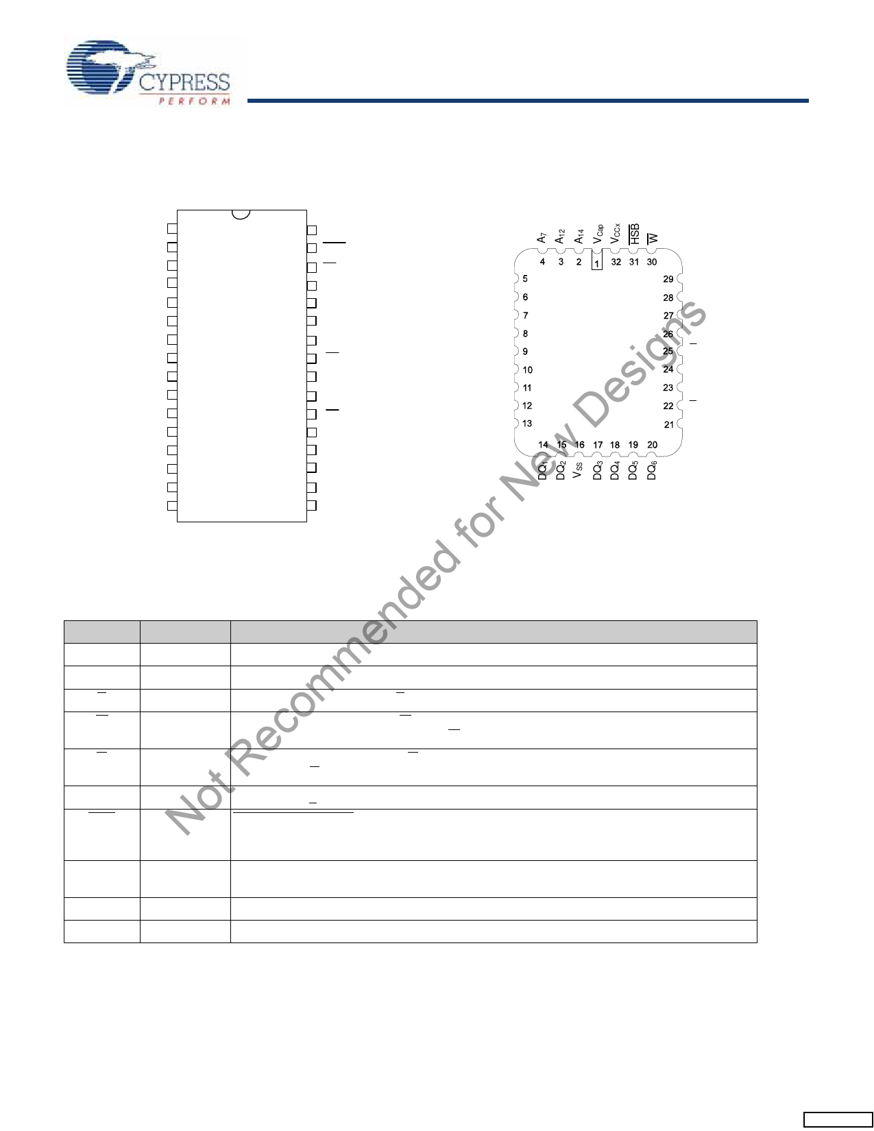
Pin Configurations
Figure 1. Pin Diagram - 32-Pin 300 Mil SOIC/CDIP
Figure 2. Pin Diagram - 32-Pin 450 Mil LCC
VCAP
1
32 VCC
A14 2
31 HSB
A12 3
30 W
A7 4
29 A13
A6
A13
A6 5
s A5 6
n A4 7
ig A3 8
NC 9
s A2 10
e A1 11
D A0 12
DQ0 13
w DQ1 14
e DQ2 15
N VSS 16
(TOP)
28 A8
27 A9
26 A11
25 G
24 NC
23 A10
22 E
21 DQ7
20 DQ6
19 DQ5
18 DQ4
17 DQ3
A5
A4
A3
NC
A2
A1
A0
DQ0
(TOP)
A8
A9
A11
G
NC
A10
E
DQ7
ed for Pin Descriptions
nd Pin Name
I/O
Description
e A14-A0
m DQ7-DQ0
m E
Input
I/O
Input
Address: The 15 address inputs select one of 32,768 bytes in the nvSRAM array.
Data: Bi-directional 8-bit data bus for accessing the nvSRAM.
Chip Enable: The active low E input selects the device.
o W
Input
Write Enable: The active low W enables data on the DQ pins to be written to the address
c location latched by the falling edge of E.
e G
Input
Output Enable: The active low G input enables the data output buffers during read cycles.
RDe-asserting G high caused the DQ pins to tristate.
t VCC
No HSB
Power Supply Power: 5.0V, +10%.
I/O
Hardware Store Busy: When low this output indicates a Store is in progress. When pulled low
external to the chip, it initiates a nonvolatile STORE operation. A weak pull up resistor keeps
this pin high if not connected. (optional connection).
VCAP
Power Supply AutoStore Capacitor: Supplies power to nvSRAM during power loss to store data from SRAM
to nonvolatile storage elements.
VSS
Power Supply Ground.
NC
No Connect Unlabeled pins have no internal connections.
Document Number: 001-52038 Rev. *C
Page 3 of 20
[+] Feedback
Share Link: 