IN74HC4051DW 查看數據表(PDF) - Integral Corp.
零件编号
产品描述 (功能)
生产厂家
IN74HC4051DW Datasheet PDF : 8 Pages
| |||
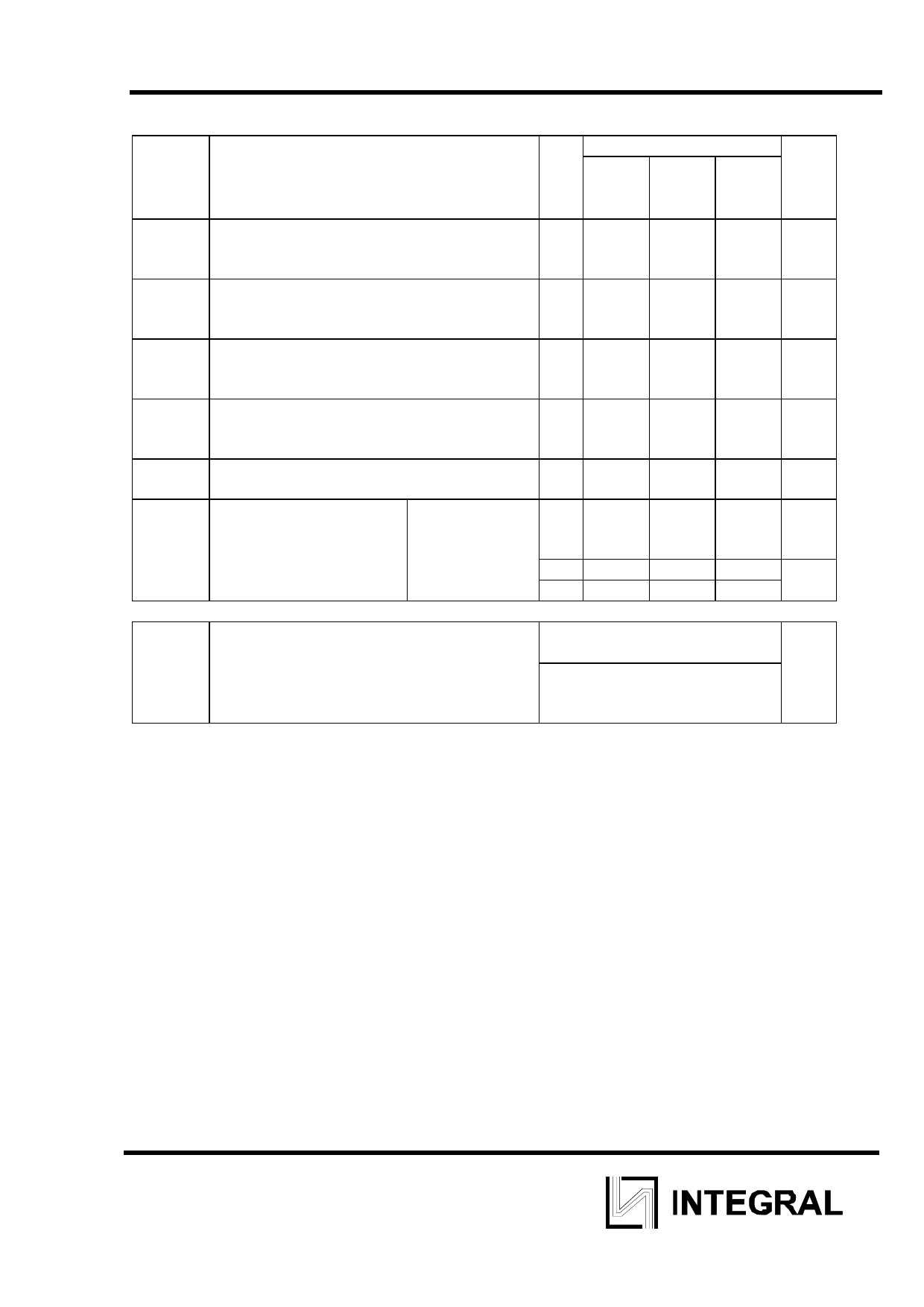
IN74HC4051
AC ELECTRICAL CHARACTERISTICS(CL=50pF,Input tr=tf=6.0 ns)
VCC
Guaranteed Limit
Symbol
Parameter
V 25 °C ≤85°C ≤125 Unit
to
°C
-55°C
tPLH, Maximum Propagation Delay, Channel- 2.0 370 465 550 ns
tPHL Select to Analog Output (Figures 8 and 4.5 74
93 110
9)
6.0 63
79
94
tPLH, Maximum Propagation Delay , Analog 2.0 60
75
90 ns
tPHL Input to Analog Output (Figures 10 and 4.5 12
15
18
11)
6.0 10
13
15
tPLZ, Maximum Propagation Delay , Enable to 2.0 290 364 430 ns
tPHZ Analog Output (Figures 12 and 13)
4.5 58
73
86
6.0 49
62
73
tPZL, Maximum Propagation Delay , Enable to 2.0 345 435 515 ns
tPZH Analog Output (Figures 12 and 13)
4.5 69
87 103
6.0 59
74
87
CIN Maximum Input Capacitance, Channel- -
10
10
10 pF
Select or Enable Inputs
CI/O Maximum Capacitance
- 35
35
35 pF
Analog All Switches
I/O
Off
Common O/I
- 130 130 130
Feedthrough
- 1.0 1.0 1.0
Power Dissipation Capacitance (Per Typical @25°C,VCC=5.0 V,
Package) (Figure 14)
VEE=0 V
CPD Used to determine the no-load dynamic
45
pF
power
consumption:
PD=CPDVCC2f+ICCVCC
4
Share Link: 