SI4735-D60-GMR(2013) 查看數據表(PDF) - Silicon Laboratories
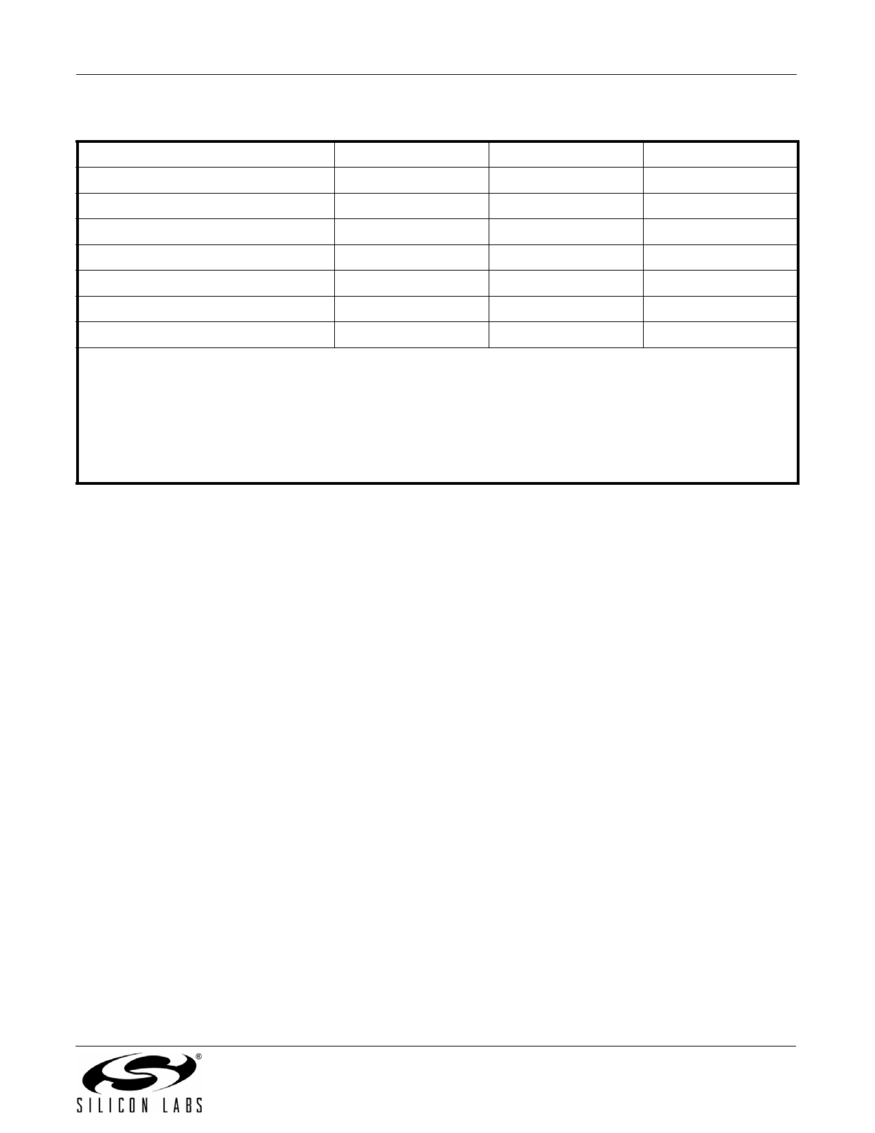
零件编号
产品描述 (功能)
生产厂家
SI4735-D60-GMR Datasheet PDF : 42 Pages
| |||
2.2. SSOP Typical Application Schematic
Si4730/31/34/35-D60
2SWLRQDO
'LJLWDO$XGLR2XW
2302'(
[%[%
&
5
'287
5
')6
5
*32'&/.
*32,17
*32
)0$QWHQQD
&
/
&
'287
')6
*32'&/.
*32,17
*32
1&
1&
)0,
5)*1'
1&
1&
$0,
2SWLRQDO
$0$LU/RRS$QWHQQD
/
/287
5287
'%<3
9$
9'
5&/.
6',2
6&/.
6(1%
567%
*1'
*1'
/287
5287
&
WR9
9$
5&/.
6',2
6&/.
6(1%
567%
WR9
9'
&
7 1
&
3
$0,
5)*1'
*32
;
&
5&/.
&
2SWLRQDO
)RU&U\VWDO26&
Notes:
1. Place C1 close to VA and C4 close to VD pin.
2. All grounds connect directly to GND plane on PCB.
3. Pins 6 and 7 are no connects, leave floating.
4. Pins 10 and 11 are unused. Tie these pins to GND.
5. To ensure proper operation and receiver performance, follow the guidelines in “AN383: Si47xx Antenna, Schematic,
Layout, and Design Guidelines.” Silicon Laboratories will evaluate schematics and layouts for qualified customers.
6. Pin 8 connects to the FM antenna interface, and pin 12 connects to the AM antenna interface.
7. Place Si473x-D60 as close as possible to antenna and keep the FMI and AMI traces as short as possible.
Rev. 1.2
19
Share Link: 