SC2434 查看數據表(PDF) - Semtech Corporation
零件编号
产品描述 (功能)
生产厂家
SC2434 Datasheet PDF : 19 Pages
| |||
SC2434
POWER MANAGEMENT
Applications Information (Cont.)
be caused by layout inductances, may alter the PWM
comparator trip point. The value of RDRP may have to be
adjusted to compensate for such parasitic effects.
Loop( s , R) H p_ccm( s , R) .H c( s )
It must be noted that the current amplifier gain is quite
precise, with greater than 80dB of Common Mode
Rejection Ratio (CMRR). Thus the droop accuracy is
primarily based upon external components tolerances. By
employing 1% current sensing element with very low
temperature coefficient, this topology is proved to be the
best comparing the schemes of using R sensing and
dson
using inductor winding resistance sensing. The accurate
drooping translates into minimum amount output bulk
capacitor needed to meet the voltage regulation specifica-
tions and the least system cost.
PO WER
STA GE
Rdrp
Vout
Ccomp
Ccomp Rcomp
C op a m
- Err_Amp
+
0
1/(R*C)
Vin/( VR*N phas e)
-1
Power St age
1/(E SRC)
Rdrp/R fb
Pol e
1/(R*C)
C o mp en sa tor
Fsw/2
-2
Zero
Verror
-1
Loop G ain
0dB
Fsw/2
-2
Programming The DC Level Of The Output Voltage
Kirchoff’s current law can be applied to the error
amplifier’s inverting input (see Fig. 1) to calculate ROS,
the DC level setting resistor. For given output voltage set
point and VID setting, the resistance can be calculated
by:
V bg
R os
V set V bg
R FB
V eo V bg
R drp
N DAC_STEP.I DAC_LSB
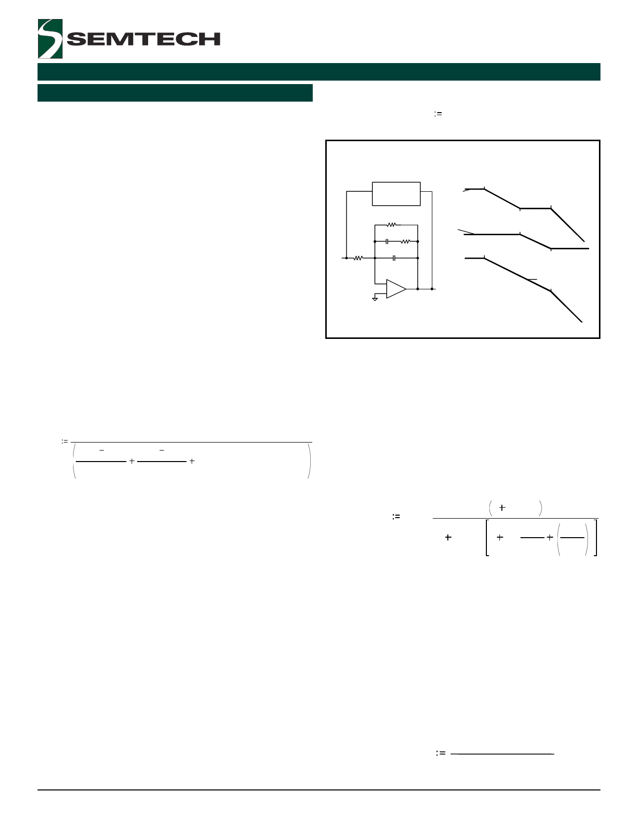
Fig. 4 - Loop gain and compensation of the current mode con-
troller.
where Copam is the equivalent internal capacitor across the
error amplifier output and the inverting input with a value
of 11pF.
The power stage transfer function under continuous
conduction mode can be approximated by:
where NDAC_STEP is the number of VID steps down from the
highest set point (VID=00000). For example, when VID
[4:1]=00100, NDAC_STEP = 4. VEO is the error amplifier
output voltage and, as a first approximation, it is equal to
1..7V. Again, VBG = Precision Reference Voltage = 1.5V.
The final value of ROS may need to be fine tuned
experimentally after the droop resistor has been chosen.
Control Loop Compensation
The current mode control yields a power supply easy to
compensate because the power stage has first order (single
pole) behavior. The SC2434 provides internal slope
compensation to avoid sub harmonic oscillation of the
current loop. The added ramp signal has 300mV peak-to-
peak amplitude and the ramp frequency is as same as
the oscillator frequency.
As depicted in Fig. 4, the gain for the voltage feedback
loop can be expressed as a product of the power stage
gain and the compensator gain:
H p_ccm( s , R)
G pwm.
(1
1 s .C.R c
s .R.C) . 1 1.5. s
π .F s
s2
π .F s
where GPWM is the low frequency gain of the power stage.
The power stage has an ESR zero, a dominant pole at
low frequency, and a pair of complex pole located at one
half of the switching frequency. The parameter used here
are defined as below:
C = output bulk capacitance
R = load resistance
RC = ESR of output bulk capacitor
FSW = switching frequency
The PWM gain is defined as:
G pwm
R ! N phase
Rsense· G CA
2005 Semtech Corp.
9
www.semtech.com
Share Link: 