N74F219AD 查看數據表(PDF) - Philips Electronics
零件编号
产品描述 (功能)
生产厂家
N74F219AD Datasheet PDF : 12 Pages
| |||
Philips Semiconductors
64-bit TTL bipolar RAM, non-inverting (3-State)
Product specification
74F219A
FEATURES
• High speed performance
• Replaces 74F219
• Address access time: 8ns max vs 28ns for 74F219
• Power dissipation: 4.3mW/bit typ
• Schottky clamp TTL
• One chip enable
• Non–Inverting outputs (for inverting outputs see 74F189A)
• 3–state outputs
• 74F219A in 150 mil wide SO is preferred options for new designs
• C3F219A in 300 mil wide SOL replaces 74F219 in existing
designs
DESCRIPTION
The 74F219A is a high speed, 64–bit RAM organized as a 16–word
by 4–bit array. Address inputs are buffered to minimize loading and
are fully decoded on chip. The outputs are in high impedance state
whenever the chip enable (CE) is high. The outputs are active only
in the READ mode (WE = high) and the output data is the
complement of the stored data.
APPLICATIONS
• Scratch pad memory
• Buffer memory
• Push down stacks
• Control store
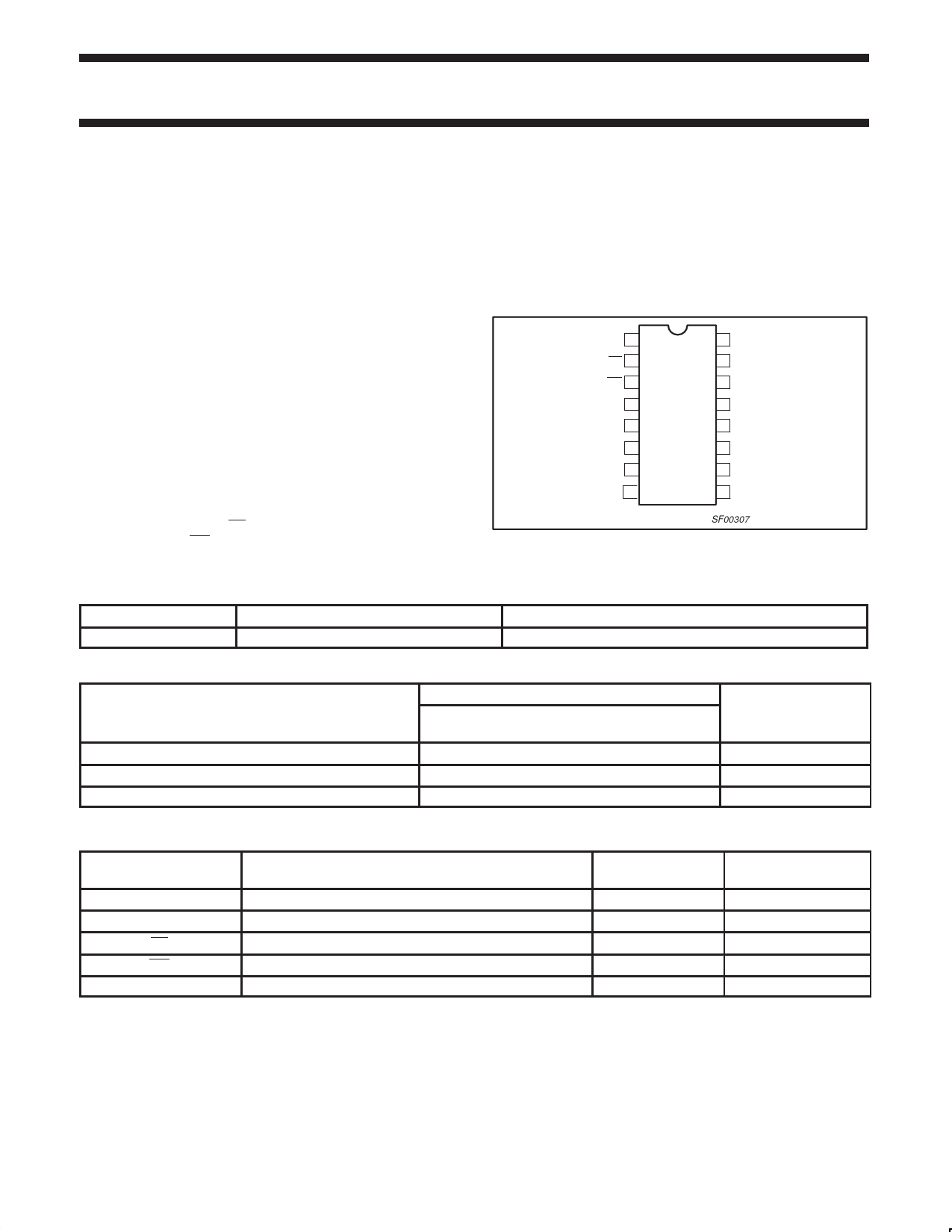
PIN CONFIGURATION
A0 1
CE 2
WE 3
D0 4
Q0 5
D1 6
Q1 7
GND 8
16 VCC
15 A1
14 A2
13 A3
12 D3
11 Q3
10 D2
9 Q2
SF00307
TYPE
74F219A
TYPICAL ACCESS TIME
5.0ns
TYPICAL SUPPLY CURRENT(TOTAL)
55mA
ORDERING INFORMATION
DESCRIPTION
16-pin plastic Dual In-line Package
16-pin plastic Small Outline (150mil)
16-pin plastic Small Outline Large (300mil)
ORDER CODE
COMMERCIAL RANGE
VCC = 5V ±10%, Tamb = 0°C to +70°C
N74F219AN
N74F219AD
C3F219AD
DRAWING NUMBER
SOT38-4
SOT109-1
SOT162–1
INPUT AND OUTPUT LOADING AND FAN OUT TABLE
PINS
DESCRIPTION
74F (U.L.)
HIGH/LOW
D0 – D3
Data inputs
1.0/1.0
A0 – A3
Address inputs
1.0/1.0
CE
Chip enable input (active low)
1.0/2.0
WE
Write enable input (active low)
1.0/2.0
Q0 – Q3
Data outputs
NOTE: One (1.0) FAST unit load is defined as: 20µA in the high state and 0.6mA in the low state.
150/40
LOAD VALUE
HIGH/LOW
20µA/0.6mA
20µA/0.6mA
20µA/1.2mA
20µA/1.2mA
3mA/24mA
1996 Jan 05
2
853-1308 16196
Share Link: 