LTC1565-31 查看數據表(PDF) - Linear Technology
零件编号
产品描述 (功能)
生产厂家
LTC1565-31 Datasheet PDF : 12 Pages
| |||
LTC1565-31
PIN FUNCTIONS
V–, V+ (Pins 4, 6): Power Supply Pins. For a single 5V
supply (Pin 4 grounded), a quality 0.1μF ceramic bypass
capacitor is required from the positive supply pin (Pin 6)
to the negative supply pin (Pin 4). The bypass should be
as close as possible to the IC. For dual supply applications
(Pin 3 is grounded), bypass Pin 6 to Pin 3 and Pin 4 to
Pin 3 with a quality 0.1μF ceramic capacitor.
The maximum voltage difference between the ground
pin (Pin 3) and the positive supply pin (Pin 6) should not
exceed 5.5V.
SHDN (Pin 5): Shutdown. When the Pin 5 voltage is low,
the LTC1565-31 goes into the current saving shutdown
mode. Pin 5 has a 4μA pull-up current. Leaving Pin 5 open
will place the LTC1565-31 in its normal operating mode.
– OUT, +OUT (Pins 7, 8): Output Pins. Pins 7 and 8 are the
filter differential output. Each pin can drive 1kΩ or 300pF
loads. The common mode voltage at the output pins is
the same as the voltage at Pin 3.
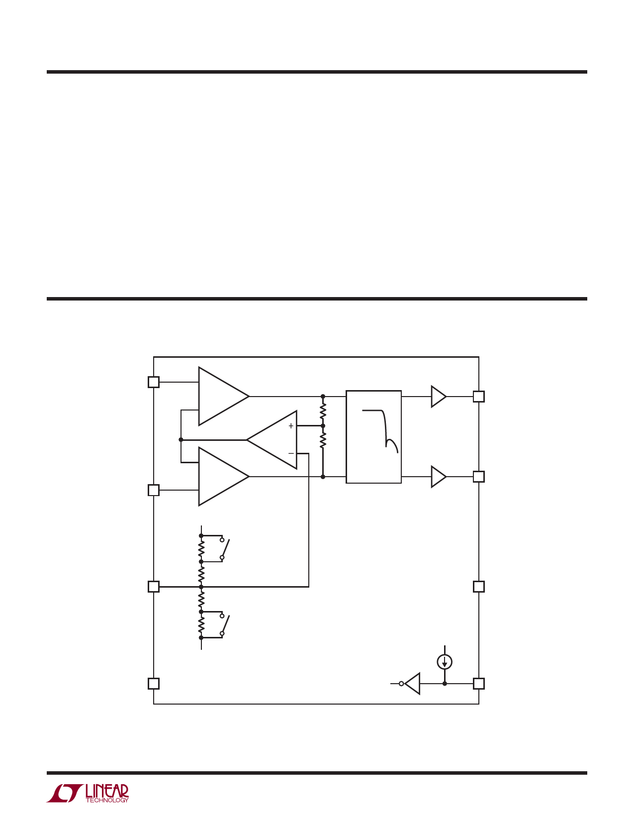
BLOCK DIAGRAM
+IN 1
–IN 2
GND 3
V– 4
+
–
–
+
INPUT BUFFERS
WITH COMMON MODE
TRANSLATION CIRCUIT
V+
~1M
SHUTDOWN
SWITCH
5k
5k
~1M
SHUTDOWN
SWITCH
V–
R
7th ORDER
LINEAR
R
PHASE
FILTER
NETWORK
SHUTDOWN
OUTPUT
BUFFER
OUTPUT
BUFFER
8 +OUT
7 –OUT
6 V+
V+
4μA
5 SHDN
1565-31 BD
156531fa
5
Share Link: 